 Quantitatively Accurate Simulations of Quantum Effects in
Semiconductor Devices
Quantitatively Accurate Simulations of Quantum Effects in
Semiconductor Devices
Quantitatively Accurate Simulations of Quantum Effects in
Semiconductor Devices
Quantitatively Accurate Simulations of Quantum Effects in
Semiconductor Devices We have made major advances in including realistic effects in the simulation of resonant-tunneling devices. The bottom line is that including realistic energy band structures resolves at least 90% of the discrepancy between simple theories and experimental I(V) curves. Random scattering accounts for the other 10%.
Conference presentation: Quantitatively Accurate Simulation of Quantum Semiconductor Devices"
This work was done as a part of the Texas Instruments-led program NEMO (for NanoElectronics MOdeling) program. The UT-Dallas work is primarily that of R. Chris Bowen (Ph.D. student, graduated 1995, presently MTS in the Semiconductor Process and Device Center, TI), and Gerhard Klimeck (postdoc, presently MTS in the Nanoelectronics Branch, soon to be Raytheon-TI Systems).
NEMO was originally conceived to ba a super-computer based comprehensive model of resonant-tunneling devices, intended in large part to address the question of how small the valley current in these devices could be. The plan was guided by the conventional wisdom of the time (1993) to the effect that inelastic scattering had a major impact on the I(V) characteristics of resonant-tunneling diodes (RTDs). After all, most of the cumulative effort expended on physical device modeling (in terms of both man-hours and computer cycles) has been directed toward getting the scattering correct, as in the popular Monte Carlo models. Also, there had been experimental observations of effects that are clearly due to scattering, such as LO phonon echoes in the I(V) curves. Note that as of 1993, no theoretical calculation had come anywhere near fitting an experimental RTD I(V) curve.
However, what one must understand is that the current density in an RTD varies exponentially with the barrier width. Thus, by making thick barriers, one can attenuate the tunneling current to any desired degree and consequently shift the otherwise negligible processes into relative prominence. This is precisely the circumstance under which LO phonon echoes were observed. In realistic device applications, one always wants to operate the device at high current density (to maximize frequency response). Consequently, engineering devices have narrow barriers, and the direct tunneling processes may predominate. These are the sort of structures that we have focussed on.
(Most of the following work appears in R. Chris Bowen, Gerhard Klimeck, Roger Lake, William R. Frensley, and Ted Moise, "Quantitative Resonant Tunneling Diode Simulation," J. Appl. Phys. 81, 7845 [1997].)
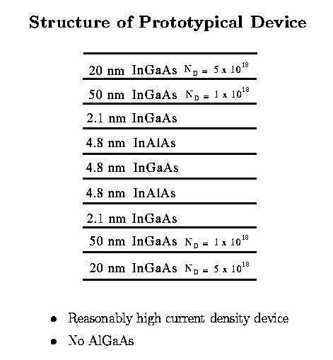
So, to begin, we will model the following structure:
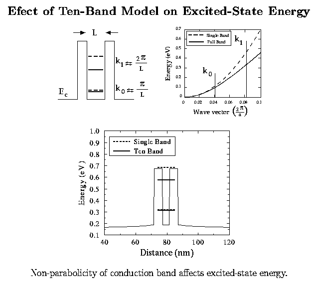
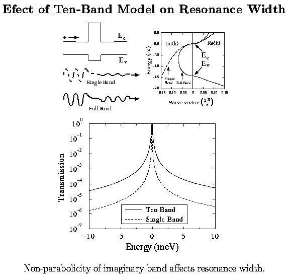
We compare the results of a single-band effective-mass calculation with a ten-band tight-binding model (ten bands are required to get an accurate fit to the conduction band structure). Observe that the current density comes much closer to the experimental data with the 10 band model.
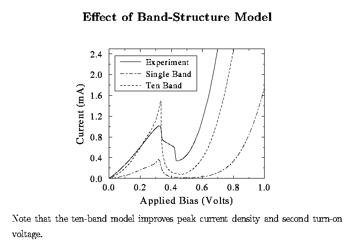
This improvement is really due to the incorporation of non-parabolicity in the conduction band, shifting the resonance energy and thus the turn-on voltage, and nonparabolicity in the imaginary band within the band gap. These effects had been described by Tom McGill, Joel Schulman, and Dave Ting, among others.
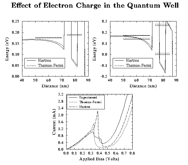
Now, the model for the charge in the cathode energy notch turns out to be a critical element of the calculation, because it determines the voltage drop across this region and thus the resonant voltage.
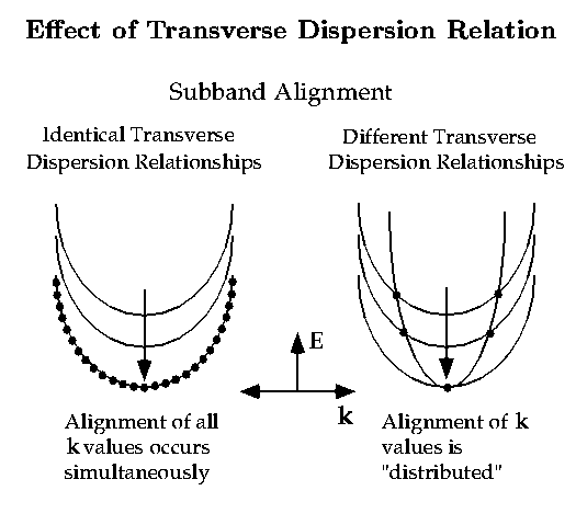
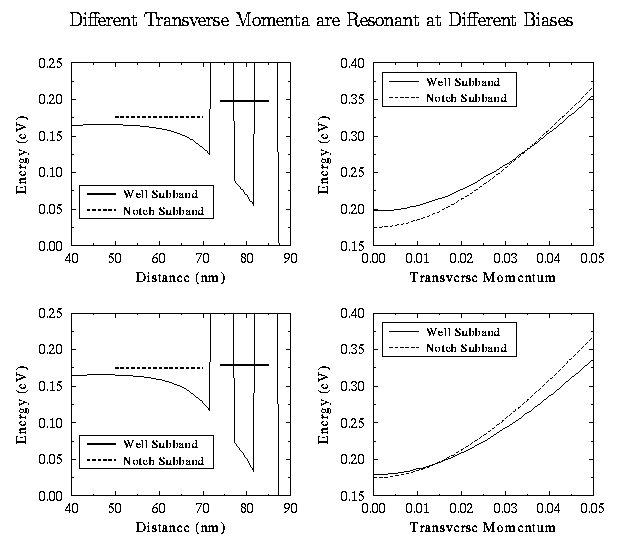
It also happens that the realistic band structure is not accurately represented by a separation-of-variables model, as illustrated below. The transverse dispersion relations do not line up at different longitudinal energies. This reduces the calculated peak current and broadens the peak of the I(V) curve. This effect was first reported by Timothy B. Boykin in Physical Review B 51, 2273 (1995).
Finally, including all of the above effects leads to this comparison with the experimental I(V) curve. The theoretical calculation overshoots the peak and undershoots the valley by about 10% of the peak current. This presumably represents the magnitude of the inelastic processes in this device. Also note that the peak and valley voltages have been accurately reproduced.
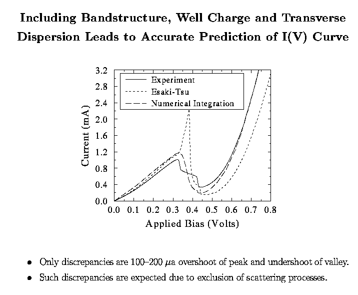
Thus, we believe that the physics of high-current density RTDs in III-V materials are now well understood.