 Vertical GaAs FET Vertical GaAs FET
 Vertical Field-Effect Transistors (VFETs) are a concept that many device engineers cannot resist. It seems so deceptively simple: rotate the channel into the vertical direction and you are defining the critical gate length with etching and deposition processes, which are capable of much higher resolution than lithography. Unfortunately these device are never simple and their performance has never lived up to expectations.
These devices were intended to be millimeter-wave amplifiers. They were made in gallium arsenide, using molecular-beam epitaxy (MBE), electron-beam lithography, and reactive-ion etching (RIE). [That qualified for a triple-buzzword score in 1983.] The devices were encapsulated in polyimide which was then etched back to expose the top-side contacts for interconnection.
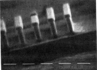
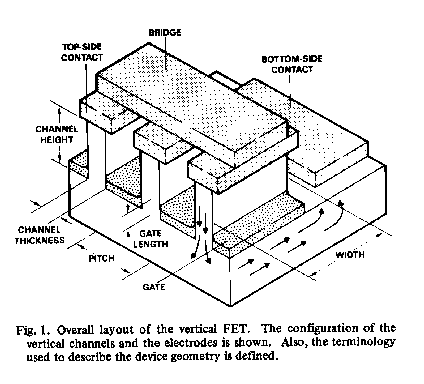
This scanning electron micrograph shows the vertical channel structure. This device had a pitch of about 1.3 micron, and vertical channel height of nearly 2 microns.
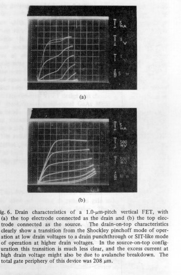
The I(V) curves showed clear evidence of short-channel effects in the form of drain punch-through. The microwave performance? Maximum oscillation frequency of about 12 GHz. The fabrication processes developed have survived as the means of making quantum-dot resonant-tunneling devices.