There are a wide variety of research projects available to PhD, MS, undergraduate, and high school students.
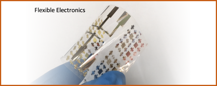
Making Flexible Metal Oxide Electronics and Transparent Conducting Electrodes Using Photons:
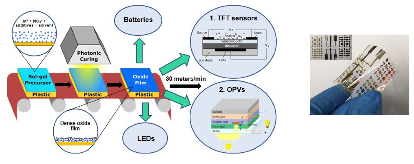
We are actively working on developing sol gel methods to fabricate electronic devices on flexible polymer substrates. To avoid degradation of the substrates, the processing temperature of every step must be kept below 250 °C, which is challenging for making high quality oxide films. We adapt combustion synthesis to keep the processing temperature low. In addition, we develop a UV method to pattern the precursor films before the calcination step, achieving two major benefits: (1) minimizing cracking of the oxide films due to the drastically different thermal expansion coefficient of the oxide and that of the polymer substrate; (2) eliminating the extra processing steps and exposure to chemicals associated with patterning using photoresist. To avoid equilibrium thermal heating (heating of the film and substrate to the same temperature) altogether, we employ photonic curing. Photonic curing uses short (20 µs – 20 ms), but very intense (up to 50 kW/cm2), pulses of broad spectrum (200 – 1200 nm) light to heat just the top surface of a sample to high temperature. Because of the low amount of energy delivered to the sample (< 100 J/cm2), the substrate is not heated significantly. This nonequilibrium process (high temperature in the film at the same time as low temperature in the substrate) allows for conversion of oxides on flexible plastic substrates. We use this process to not only convert solution-deposited ZrO2 films on plastic substrates, but also to pattern them by taking advantage of the varying optical and thermal response of patterns on the substrate beneath the oxide film. Most importantly, because this process is both fast and is compatible with flexible substrates, it can be used in large-scale roll-to-roll processing (similar to a newspaper printing press) of oxide electronics at speeds up to 30 meters/min.
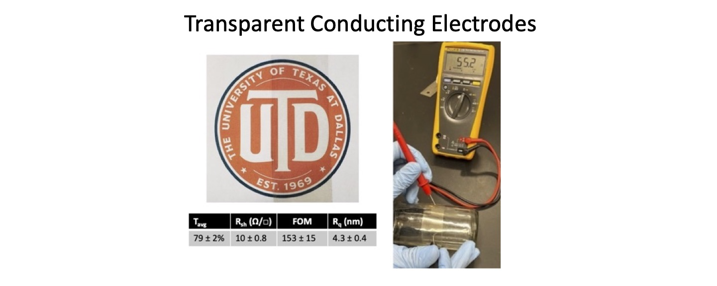
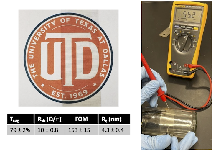
We recently use blade coating and photonic curing to fabricate hybrid transparent conducting electrodes that consist of metal bus lines, AgNWs, and IZO layer on PET. We have successfully fabricated working perovskite solar cells on them.
Key Publications:
- T. B. Daunis, G. Futierrez-Heredia, O. Rodriguez-Lopez, J. Wang, W. E. Voit, and J. W. P. Hsu, "Solution-deposited Al2O3 dielectric towards Fully-patterned Thin Film Transistors on Shape Memory Polymer"; Proceedings of SPIE, Oxide-based Materials and Devices VIII, 1010>, 101051Z (2017)
- J. Wang, T. B. Daunis, L. Cheng, B. Zhang, J. Kim, and J. W. P. Hsu, “Combustion Synthesis of P-type Transparent Conducting CuCrO2+x and Cu:CrOx Thin Films at 180°C,” ACS Applied Materials and Interfaces 10, 3732-3738 (2018)
- T. B. Daunis, D. Barrera, G. Gutierrez-Heredia, O. Rodriguez-Lopez, J. Wang, W. E. Voit, and J. W. P. Hsu, “Photochemically Patterned High-Performance Solution-Processed Oxide Devices on Shape Memory Polymer,” J. Mater. Res. 33, 2454-2462 (2018)
- T. B. Daunis, J. M. H. Tran, and J. W. P. Hsu, “Effects of Environmental Water Absorption by Solution-Deposited Al2O3 Gate Dielectrics on Thin Film Transistor Performance and Mobility, ” ACS Appl. Mater. Interfaces 10 (46), 39435-39440 (2018)
- T. B. Daunis, K. A. Schroder, and J. W. P. Hsu, “Photonic Curing of Solution-Deposited ZrO2 Dielectric on PEN: A Path Towards High-Throughput Processing of Oxide Electronics,” npj Flexible Electronics 4, 7 (2020)
- T. B. Daunis, W. Xu, S. Thampy, M. Valdez, and J. W. P. Hsu, “Effects of Atmosphere Composition During Direct Ultraviolet-Light Patterning of Solution-Deposited In2O3 Thin Film Transistors,” Thin Solid Films 733, 138829 (2021)
- R. T. Piper, W. Xu, and J. W. P. Hsu, “Silver Nanowire-Indium Zinc Oxide Composite Flexible Transparent Conducting Electrodes Made by Spin-coating and Photonic Curing,” MRS Adv. 8, 177-182 (2023)
Flexible Halide Perovskite Solar Cells and Light Emitting Diodes:
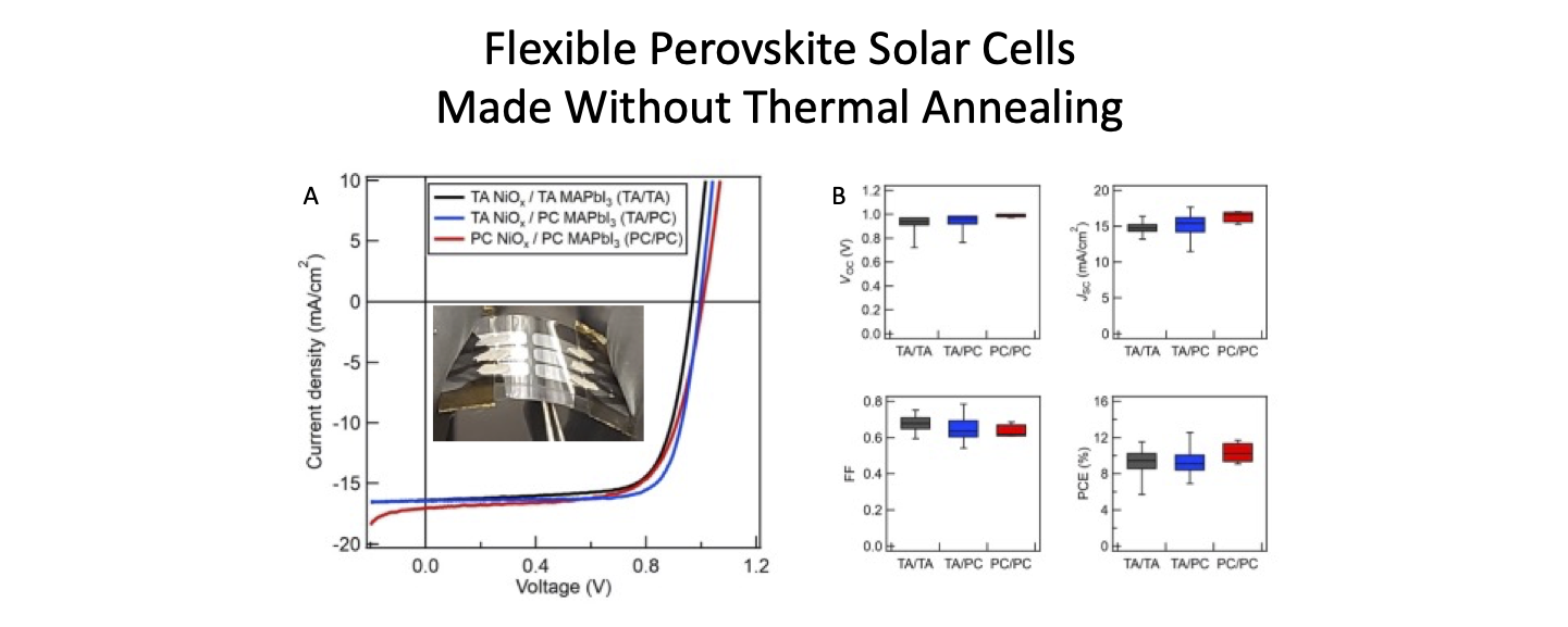
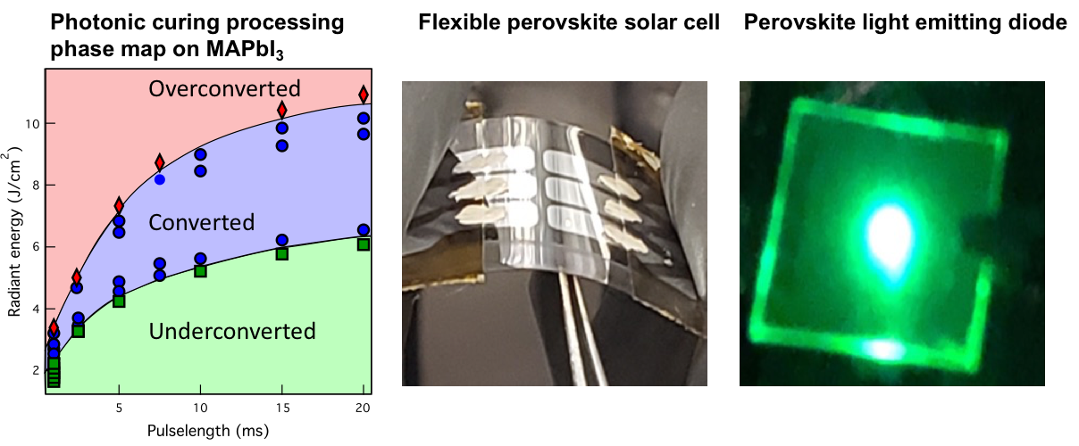
Halide perovskite has emerged as a revolutionary photovoltaics material with its excellent optoelectronic properties and inexpensive solution-processability. We are working on a variety of flexible perovskite devices, including perovskite solar cells (PSCs) and perovskite light-emitting diodes (PLEDs). To increase the throughput of fabrication, we utilize photonic curing to replace conventional thermal annealing to crystallize the perovskite materials. We successfully photonically cure MAPbI3 as the active layer in flexible PSCs. The processing time for MAPbI3 is reduced to 20 ms, which is a 30,000-fold improvement compared to 10-min-thermal annealing. This process is not only used in PSCs fabrication, but we also use it to convert CsPbBr3 for PLEDs.
Key Publications:
- W. Xu, T. B. Daunis, R. T. Piper, and J. W. P. Hsu, “Effects of Photonic Curing Processing Conditions on MAPbI3 Film Properties and Solar Cell Performance,” ACS Appl. Energy Mater. 3 (9), 8636-8645 (2020)
- R. T. Piper, T. B. Daunis, W. Xu, K. A. Schroder, and J. W. P. Hsu, “Photonic Curing of Nickel Oxide Transport Layer and Perovskite Active Layer for Flexible Perovskite Solar Cells: A Path towards High-throughput Manufacturing,” Front. Energy Res. 9, 640960 (2021)
- Team Lights Promising Way to Future of Solar Panel Production
- R. T. Piper, W. Xu, and J. W. P. Hsu, “Effects of Optical and Electrical Properties of ITO Coated Willow Glass on Photonic Curing for Upscaling Perovskite Solar Cell Manufacturing,” IEEE J. Photovol 12 (3), 722-727 (2022)
- W. Xu, R. T. Piper, and J. W. P. Hsu, “Elucidating diiodomethane-induced improvement in photonically cured MAPbI3 solar cells,” ACS Appl. Energy Mater. 5 (6), 7328-7334 (2022)
- W. Xu, J. C. Bonner, R. T. Piper, and J. W. P. Hsu, “Effects of Residual DMSO Adduct on Photonically Cured MAPbI3 Solar Cells,” J. Phys. Chem. C in Virtual Special Issue “The Physics and Chemistry of Perovskites ” (2023)
Photonic Curing of Halide Perovskite Films
Incorporating Machine Learning for Materials Synthesis and Processing:
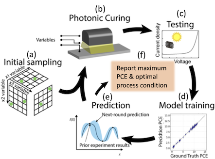
Optimization is inherent in materials synthesis and processing because the goal is often to find the “best” certain properties. However, acquiring experimental data is time-consuming and expensive, and there are many variables (explicit or hidden) that can affect the desired outcome. Bayesian optimization (BO) with Gaussian process is particularly suitable for small data sets and “black box” relation between the inputs and the output. We build a model based on the data from a few initial experiments that judiciously sample the multi-dimensional input space and then use the prediction to guide us on where in the input space to acquire the next round of experiments depending on the goal of the experiment. The new data are then added to existing data to refine the model and prediction. The iterative process is repeated until the desired outcome is achieved or the experimental resource is exhausted.
Key Publications:
- W. Xu, Z. Liu, R. T. Piper, and J. W. P. Hsu, “Bayesian Optimization of Photonic Curing Process for Flexible Perovskite Photovoltaic Devices,” Solar Energy Mater. Solar Cells 249, 112055 (2023)
Interfacial Reaction between Halide Perovskite and Metal Oxide transport Layer:
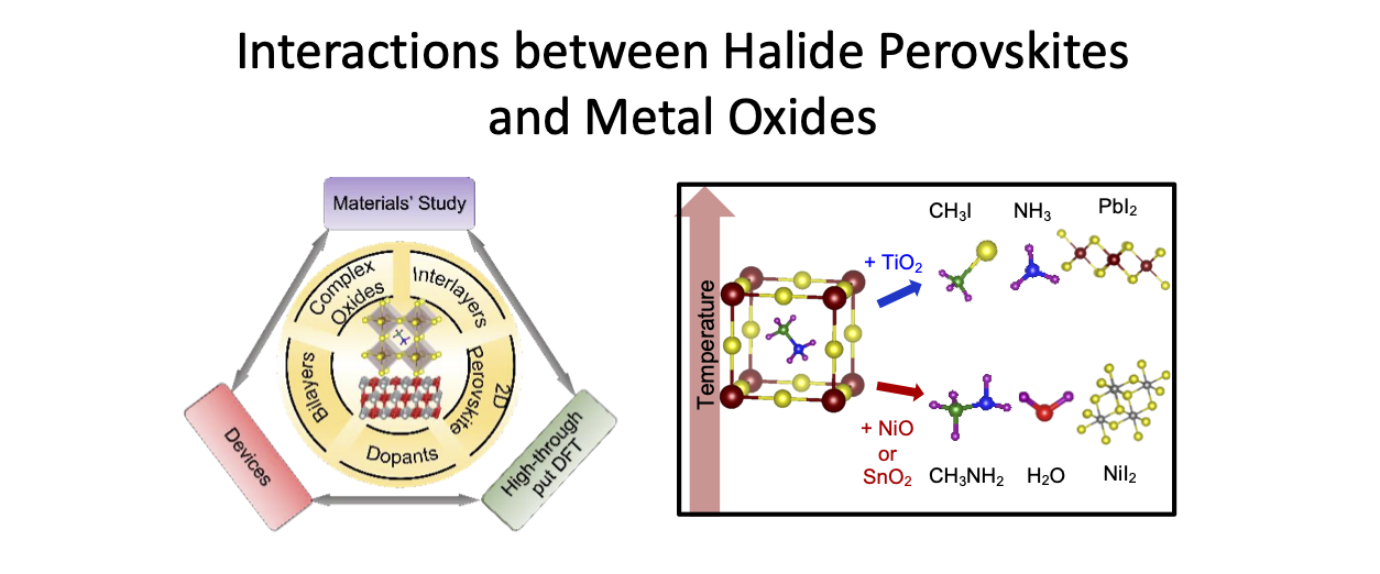
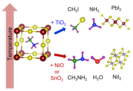
Organic-inorganic halide perovskites have demonstrated superior optoelectronic properties, making them great candidates in various applications. In particular, perovskite solar cells (PSCs) have leapfrogged several technologies in power conversion efficiencies. For these halide perovskite materials to become viable technologies, stability is a critical issue. Many works have examined the environmental stabilities of PSCs, in particular due to oxygen, humidity, and UV light. To date the intrinsic stability studies focused on the degradation mechanism of halide perovskites by themselves, i.e. bulk decomposition. However, in devices, the halide perovskite is in contact with other materials. With improved packaging the detriment of environment can be greatly reduced, but the interactions between halide perovskites and contact materials cannot be eliminated as contact layers are integral to the devices. Thus, understanding possible reactions from interfacial interaction is critical to address the intrinsic stability of perovskite devices. We examine the thermal stability and degradation pathways in MAPbI3 and FAPbI3, when in contact with commonly used metal oxide transport layer materials—NiO, TiO2, or SnO2, using a combined temperature programmed desorption-mass spectrometry-Fourier transform infrared spectroscopy (TPD-MS-FTIR) technique. The simultaneous MS and FTIR measurements are essential for unambiguous identification of evolved gases, because MS detects ions and are complicated by ionization and fragmentation probabilities while FTIR measures the characteristic vibrational frequencies associated with specific moieties in neutral molecules, but often exhibits similar or overlapping spectra. The experimental results are augmented by thermodynamic calculations and density functional theory (DFT) modelling.
Key Publications:
- S. Thampy, B. Zhang, K.-H. Hong, K. J. Cho and J. W. P. Hsu, “Altered Stability and Degradation Pathway of CH3NH3PbI3 in Contact with Metal Oxide,” ACS Energy Lett. 5, 1147-1152 (2020)
- S. Thampy, B. Zhang, J.-G. Park, K.-H. Hong, and J. W. P. Hsu, “Bulk and Interfacial Decomposition of Formamidinium Iodide (HC(NH2)2) in Contact with Metal Oxide,” Mater. Adv. 1, 3349-3357 (2020)
- S. Thampy, W. Xu, and J. W. P. Hsu,“Metal Oxide Induced Instability and Its Mitigation in Halide Perovskite Solar Cells,” J. Phys. Chem. Lett. 12, 8495-8506 (2021)
Solar Cell Fabrication, Testing, and Device Physics Studies:
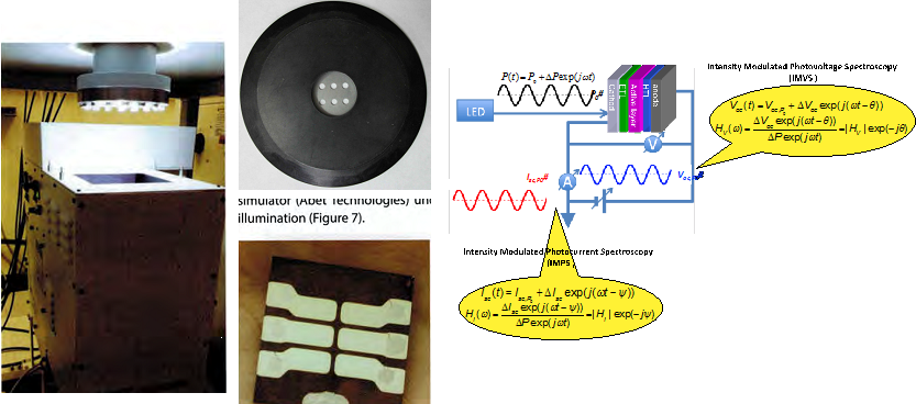
Students fabricate and test solar cells using state-of-the-art facilities. Device power conversion efficiency will be measured in the glove box using an AAA solar simulator. For other measurements, the solar cell is protected from air and moisture in an O-ring shield housing. External quantum efficiency (EQE) measurements reveal the conversion fraction from photon to charged carriers, as well as probing the existence of sub-band gap charge transfer states. Impedance spectroscopy as a function of bias, frequency, and illumination intensity provides information on background doping level, deep trap energetics, transport, storage capacity, and recombination rate and mechanism of photo-generated charges. Numerical simulations complement experiments to elucidate the physical origin of different device behavior. These studies enable us to pinpoint the areas that need improvement in the current devices in order to design more efficient solar cells.
Key Publications:
- S. R. Cowan, J. Wang, J. Yi, Y.-J. Lee, D. C. Olson, and J. W. P. Hsu,"Intensity and Wavelength Dependence of Bimolecular Recombination in P3HT:PCBM Solar Cells: a White-Light Biased External Quantum Efficiency Study," J. Appl. Phys. 113, 154504 (2013)
- L. Xu, J. Wang, Y.-J. Lee, and J. W. P. Hsu, "Relating Non-geminate Recombination to Charge-Transfer States in Bulk Heterojunction Organic Photovoltaic Devices"; J. Phys. Chem. C 119, 19628-19633 (2015)
- J. Wang, L. Xu, Y.-J. Lee, M. De Anda Villa, A. V. Malko, and J. W. P. Hsu,"Effects of Contact-Induced Doping on the Behaviors of Organic Photovoltaic Devices," Nano Letters 15, 7627-7632 (2015)
- L. Xu, J. Wang, M. De Anda Villa, T. B. Daunis, Yun-Ju Lee, A. V. Malko, and J. W. P. Hsu,"Quantitative Analyses of Competing Photocurrent Generation Mechanisms in Fullerene-based Organic Photovoltaics," J. Phys. Chem. C 120, 16470-16477 (2016)
- L. Xu, J. Wang, and J. W. P. Hsu,"Transport Effects on Capacitance-Frequency Analysis for Defect Characterization in Organic Photovoltaic Devices," Phys. Rev. Applied 6, 064020 (2016)
- J. Wang, L. Xu, B. Zhang, Y.-J. Lee, and J. W. P. Hsu,"N-type Doping Induced by Electron Transport Layer in Organic Photovoltaic Devices," Adv. Electron. Mater. 3, 1600458 (2017)
- L. N. S. Murthy, D. Barrera, A. Gadh, L. Xu, F.-Y. Cao, C.-C. Tseng, Y.-J. Cheng, and J. W. P. Hsu, “Probing Defect States in Organic Polymers and Bulk Heterojunctions using Surface Photovoltage Spectroscopy,” J. Phys. Chem. C 123, 10795-10801 (2019)
Carrier Transport Mechanism in Dilute Donor Organic Solar Cells (OSCs):
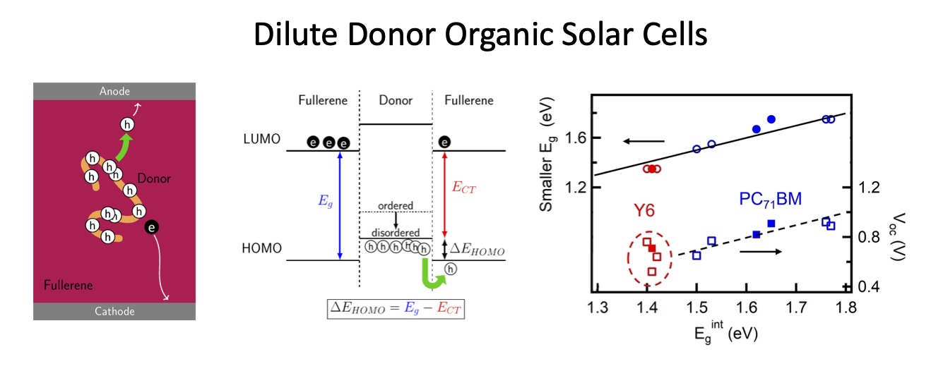
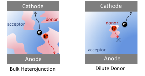
Recently, a different kind of OSC system, which circumvents the tradeoff between Jsc and Voc, has gained attention. Fullerene-based OSCs, also called dilute-donor OSCs, contain only a small amount of donor material embedded in the fullerene matrix and show a substantial Jsc while maintaining a high Voc. Large Voc was first observed in pure C60 devices and remains high even when a small amount of donor molecules is included. Furthermore, the Voc value is independent of donor molecule concentration and has been attributed to the formation of a Schottky barrier at the fullerene/anode contact or a reduction in recombination of free charge carriers. The more curious observation is the substantial Jsc increase with even a small amount of donor molecules in the dilute-donor systems. This finding is not restricted to specific materials. In a BHJ system, donor-rich and acceptor-rich domains provide percolating paths for holes and electrons to transport to their respective electrodes. In contrast, in a dilute-donor active layer, due to the low concentration, individual donor molecules are likely to be entirely surrounded by acceptors. During exciton separation, holes are transferred from the acceptor to donor and are trapped on the donor domains without percolation pathways to the anode. The scientific puzzle is why does Jsc increase so much with addition of a small amount of donor?
Key Publications:
- L. Xu, J. Wang, M. De Anda Villa, T. B. Daunis, Yun-Ju Lee, A. V. Malko, and J. W. P. Hsu, "Quantitative Analyses of Competing Photocurrent Generation Mechanisms in Fullerene-based Organic Photovoltaics," J. Phys. Chem. C 120, 16470-16477 (2016)
- T. Albes, L. Xu, J. Wang, J. W. P. Hsu, and A. Gagliardi, “The Origin of Photocurrent in Fullerene-based Solar Cells,” J. Phys. Chem. C 122, 15140-15148 (2018)
- L. N. S. Murthy, B. Zhang, and J. W. P. Hsu, “Effect of Device Architecture in Fullerene-based Organic Solar Cells,” J. Phys. Chem. C 124 (24), 12982-12989 (2020)
- W. Kaiser, L. N. S. Murthy, C.-L. Chung, K.-T. Wong, J. W. P. Hsu, and A. Gagliardi, “Origin of Hole Transport in Small Molecule Dilute Donor Solar Cells,” Adv. Energy & Sustainability Res. 2 (3), 2000042 (2021)
- L. N. S. Murthy, A. A. Kramer, B. Zhang, J.-M. Su, Y.-S. Chen, K.-T. Wong, W. G. Vandenberghe, and J. W. P. Hsu, “Tailoring Thienothiophene Molecules as Donors to Study Photocurrent Generation in Fullerene-Based Organic Solar Cells,” Org. Electron. 92, 106137 (2021)
- B. Zhang, L. N. S. Murthy, A. Mishra, M. Bowers, C.-L. Chung, J. Du, M. C. Stefan, K.-T. Wong, J. D. Slinker, and J. W. P. Hsu, “Re-examining Open-circuit Voltage in Dilute-donor Organic Photovoltaics,” J. Phys. Chem. C 126 (22), 9275-9283 (2022)
- B. Zhang, J. C. Bonner, W. Xu, R. T. Piper, L. N. S. Murthy, and J. W. P. Hsu, "Contributions of Charge Generation versus Transport to Photocurrent in Dilute-donor Organic Solar Cells with Non-fullerene Acceptors", J. Phys. Chem. C. 126 (49), 20793-20799 (2022)
- A. Kramer, W. Kaiser, B. Zhang, L. N. S. Murthy, A. Gagliardi, J. W. P. Hsu, and W. G. Vandenberghe, “Understanding Morphology Effects on Fill Factor Losses in Dilute-Donor Organic Solar Cells,” Nano Energy 103 (A), 107793 (2022)
Past Projects
Solution synthesis of nanomaterials:
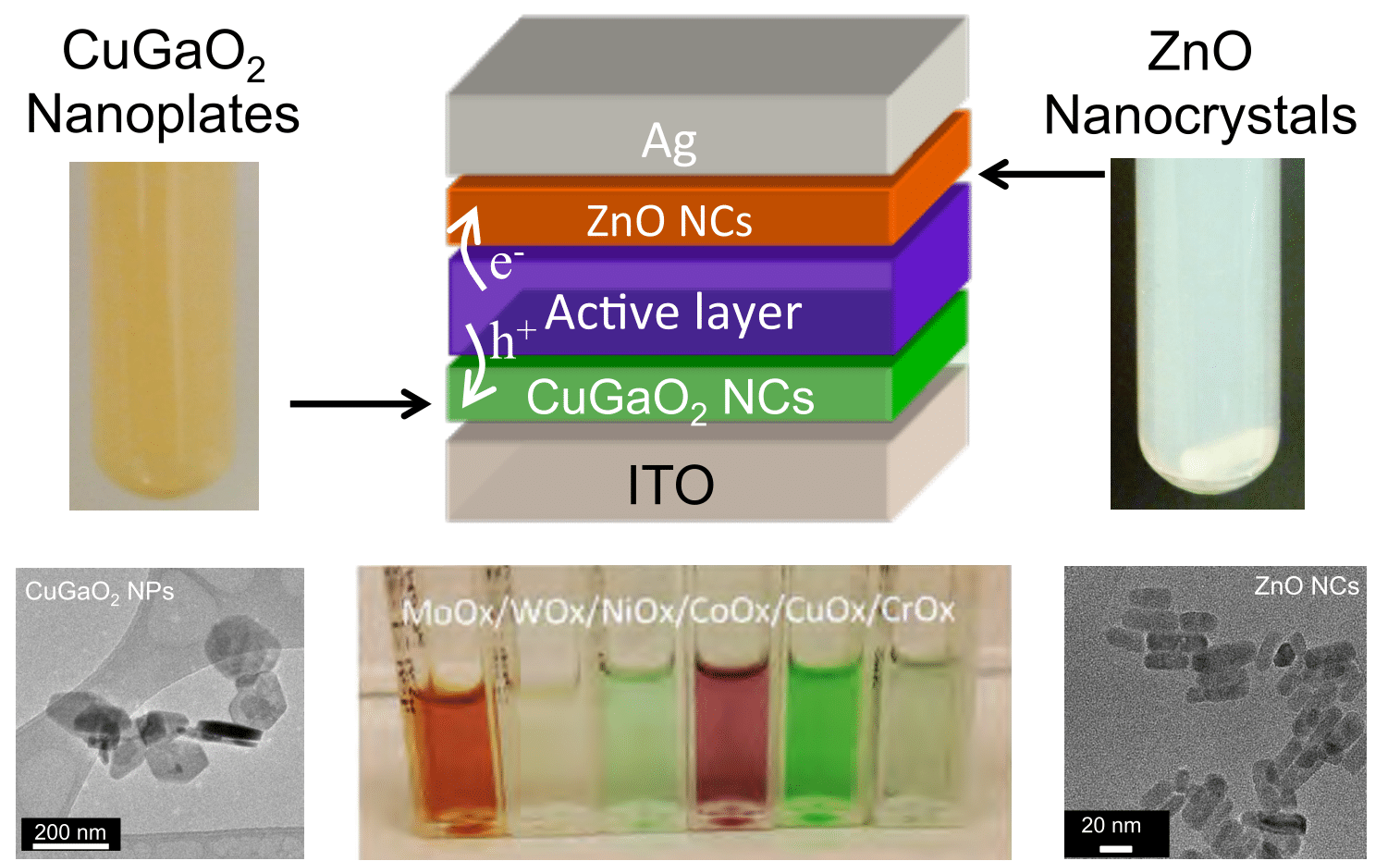
We primarily synthesize metal oxide nanomaterials using microwave, hydrothermal, and precipitation-calcination techniques. Some examples of binary oxides are ZnO, MoO3, WoO3, NiO, and CoOx. In addition, we synthesize p-type delafossite CuMO2 (M = Ga, Cr, Fe, Mn, etc.) nanocrystals, Mn- and Fe- perovskites such as SmMnO3, and Mn- and Fe- mullite compounds like AMn2O5 (A = Y, Sm, Gd, Pr, or Bi). We also synthesized transition metal dichalcogenide (TMD) compounds, e.g. MoS2, MoSe2, WS2, and WSe2, either directly from precursors or via liquid exfoliation of bulk minerals. Through synthesis conditions, we control their size, band gap, work function, or crystallinity. Applications of these materials include transport layers for organic and perovskite photovoltaics and small molecule catalysis.
Key Publications:
- Y.-J. Lee, J. Yi, G. F. Gao, H. Koerner, K. Park, J. Wang, K. Luo, R. A. Vaia, and J. W. P. Hsu,"Low-temperature Solution Processed Molybdenum Oxide Nanoparticle Hole Transport Layers for Organic Photovoltaic Devices," Adv. Energy Mater. 2, 1193-1197 (2012)
- J. Wang, Y.-J. Lee, and J. W. P. Hsu,"One-step Synthesis of ZnO Nanocrystals in n-butanol with Bandgap Control: Applications in Hybrid and Organic Photovoltaic Devices," J. Phys. Chem. C 118, 18417-18423 (2014)
- J. Wang, Y.-J. Lee, and J. W. P. Hsu,"Sub-10 nm Copper Chromium Oxide Nanocrystals as Solution Processed p-Type Hole Transport Layer for Organic Solar Cells," J. Mater. Chem. C 4, 3607-3613 (2016)
- S. Thampy , V. Ibarra , Y.-J. Lee , G. McCool , K. Cho , and J. W. P. Hsu,"Effect of Synthesis Conditions on Structure and NO Adsorption Properties of SmMn2O5," Appl. Surf. Sci. 385, 490-497 (2016)
- D. Barrera, Q. Wang, Y.-J. Lee, L. Cheng, M. J. Kim, J. Kim, and J. W. P. Hsu,"Solution Synthesis of Few-layer 2H MX2 (M=Mo,W;X=S,Se)," J. Mater. Chem. C 5, 2859-2864 (2017)
- W. A. Dunlap-Shohl, T. B. Daunis, X. Wang, J. Wang, B. Zhang, D. Barrera, Y. Yan, J. W. P. Hsu, and D. B. Mitzi, “Room-temperature Fabircation of a Delafossite CuCrO2 Hole Transport Layer for Perovskite Solar Cells,” J. Mater. Chem. A 6, 469-277 (2018)
- B. Zhang, S. Thampy, W. Dunlap-Shohl, W. Xu, Y. Zheng, F.-Y. Cao, Y.-J. Cheng, A. V. Malko, D. B. Mitzi, and J. W. P. Hsu, “Mg Doped CuCrO2 as Efficient Hole Transport Layers for Organic and Perovskite Solar Cells,” Nanomaterials 9 (10), 1311-1321 (2019)
Video on Copper Gallium Oxide Nanoplate Synthesis: J. Wang, V. Ibarra, D. Barrera, L. Xu, Y.-J. Lee, and J. W. P. Hsu,"Solution Synthesized p-Type Copper Gallium Oxide Nanoplates as Hole Transport Layer for Organic Photovoltaic Devices," J. Phys. Chem. Lett. 6, 1071-1075 (2015) 10.1021/acs.jpclett.5b00236
Combustion Synthesis
Without Glycine
|
With Glycine
|
Mullite-type oxides with Earth-abundant elements to replace Pt-group metal catalysts:
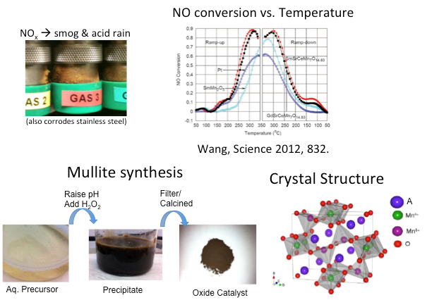
In 2015 the World was shocked to find out that automaker Volkswagen used software to disable nitric and nitrogen oxide (NOx) trap in their diesel cars in order to boost up fuel efficiency, emitting up to 40 times higher NOx exhaust than the permitted level. Today diesel automobiles comprise more than 50% of the European market because diesel engines are more fuel-efficient than gasoline engines. However, diesel exhaust contains various pollutants, including NOx, carbon monoxide (CO), and particulate matter (PM), which are harmful to human health and damaging to the environment. In the exhaust gas the NOx is composed of 90% NO and 10% NO2, but equal amount of NO and NO2 is needed to achieve efficient reduction reaction to generate N2 and O2. Hence an NO oxidation reaction is needed, which requires catalysis at low temperatures. Current technologies use platinum group metals (PGMs) as NO oxidation catalysts. However, the extreme scarcity of PGMs (~1 ppb in Earth crust) makes the cost unsustainable. Hence, it is valuable to develop inexpensive catalysts using Earth-abundant elements. We have been collaborating with Prof. Cho's group and Prof. Chabal's group on developing SmMn2O5 mullite and related compounds for this application. The project involves materials synthesis and characterization, surface reaction studies, and DFT calculations.
Key Publications:
- C. Li, S. Thampy, Y. Zheng, M. Kweun, Y. Ren, J. Y. Chan, H. Kim, M. Cho, Y. Y. Kim, J. W.P. Hsu, and K. Cho,"Thermal Stability of Mullite RMn2O5 (R = Bi, Y, Gd, Pr, or Sm): Combined Density Functional Theory and Experimental Study," J. Phys.: Condens. Matter 28, 125602 (2016) 10.1088/0953-8984/28/12/125602
- S. Thampy, Y. Zheng, S, Dillon, C. Liu, Y. Jangjou, Y.-J. Lee, W. S. Epling, K. Xiong, Y. J. Chabal, K. Cho, and J. W. P. Hsu,"Superior Catalytic Performance of Mn-Mullite over Mn-Perovskite for NO Oxidation," Catalysis Today 310, 195-201 (2018)
- S. Thampy, N. Ashburn, T. J. Martin, C. Li, Y. Zheng, J. Y. Chan, K. Cho, and J. W. P. Hsu, “Effect of R-site Element on Crystalline Phase and Thermal Stability of Fe Substituted Mn-Mullite Oxides: R2(Mn1-xFex)4O10-δ (R = Y, Sm or Bi; x = 0, 0.5, 1),” RSC Advances 8, 28-37 (2018)
- S. Thampy, N. Ashburn, S. Dillon, C. Liu, K. Xiong, E. C. Mattson, Y. Zheng, Y. J. Chabal, K. Cho, and J. W. P. Hsu, “Critical Role of Mullite-type Oxides' Surface Chemistry on Catalytic NO Oxidation Performance, ” J. Phys. Chem. C 123, 5385-5393 (2019)
- S. Thampy, N. Ashburn, C. Liu, K. Xiong, S. Dillon, Y. Zheng, Y. J. Chabal, K. Cho, and J. W. P. Hsu, “Superior Low-temperature NO Catalytic Performance of PrMn2O5 over SmMn2O5 Mullite-type Catalysts, ” Catal. Sci. Technol. 9, 2758-2766 (2019)
- Y. Zheng, S. Thampy, N. Ashburn, S. Dillon, L. Wang, Y. Jangjou, K. Tan, F. Kong, Y. Nie, M. J. Kim, W. S. Epling, Y. J. Chabal, J. W. P. Hsu, and K. Cho,“Stable and Active Oxidation Catalysis by Cooperative Lattice Oxygen Redox on SmMn2O5 Mullite Surface,” J. Am. Chem. Soc. 141, 10722-10728 (2019)
- N. Ashburn, Y. Zheng, S. Thampy, S. Dillon, Y. J. Chabal, J. W. P. Hsu, and K. Cho, “Comparative Experimental-Theoretical Study on the Reliability of Molecule Interactions with Transition Metal Oxide Surfaces,” Appl. Mater. Interfaces 11, 30460-30469 (2019)
- S. Thampy, N. Ashburn, S. Dillon, Y. J. Chabal, K. J. Cho, and J. W. P. Hsu, “Role of Surface Oxygen Vacancies in Intermediate Formation on Mullite-type Oxides upon NO Adsorption,” J. Phys. Chem. C 124 (29), 15913-15919 (2020)
- S. Thampy, N. Ashburn, K. Cho, and J. W. P. Hsu, “Earth-Abundant Transition Metal Based Mullite-type Oxide Catalysts for Heterogeneous Oxidation Reactions,” Adv. Energy & Sustainability Res. 2 (4), 202000075 (2021)
Polymer Nanocomposites for High Data Rate Communications:
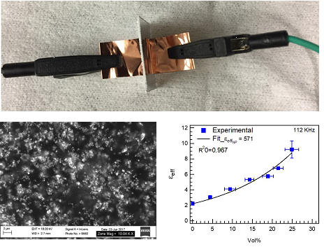
High-data-rate communications have pushed carrier frequencies up to the millimeter-wave frequencies and are now ubiquitously demanded in a wide variety of sectors. A major roadblock to the deployment of high-speed electronic systems is the lack of low-loss interconnects for signal transmission. Collaborating with Texas Instruments Kirby Lab, we are investigating polymer nanocomposites for on-chip and chip-to-chip communications at 50 to 300 GHz. In these applications, having low loss is the most important criteria since the total signal loss is proportional to the product of frequency and loss tangent. Loss mechanisms relevant at these high frequencies are currently unknown. We synthesize and characterize the nanocomposite materials, and characterize their dielectric properties: below 1 MHz by measuring capacitors and between 140 and 220 GHz through waveguide characterization.
Key Publications:
- M. D. Womble, J. Herbsommer, Y.-J. Lee, and J. W. P. Hsu,"Understanding the Source of Dielectric Loss in Titania/Polypropolyne Nanocomposites up to 220 GHz," Proceedings of SPIE, Optical Interconnects XVII, 10109, 1010908 (2017)
- M. D. Womble, J. Herbsommer, Y.-J. Lee, and J. W. P. Hsu, “Effects of TiO2 Nanoparticle Size and Concentration on Dielectric Properties of Polypropylene Nanocomposites,” J. Mater. Sci. 53 (12), 9149-9159 (2018)


