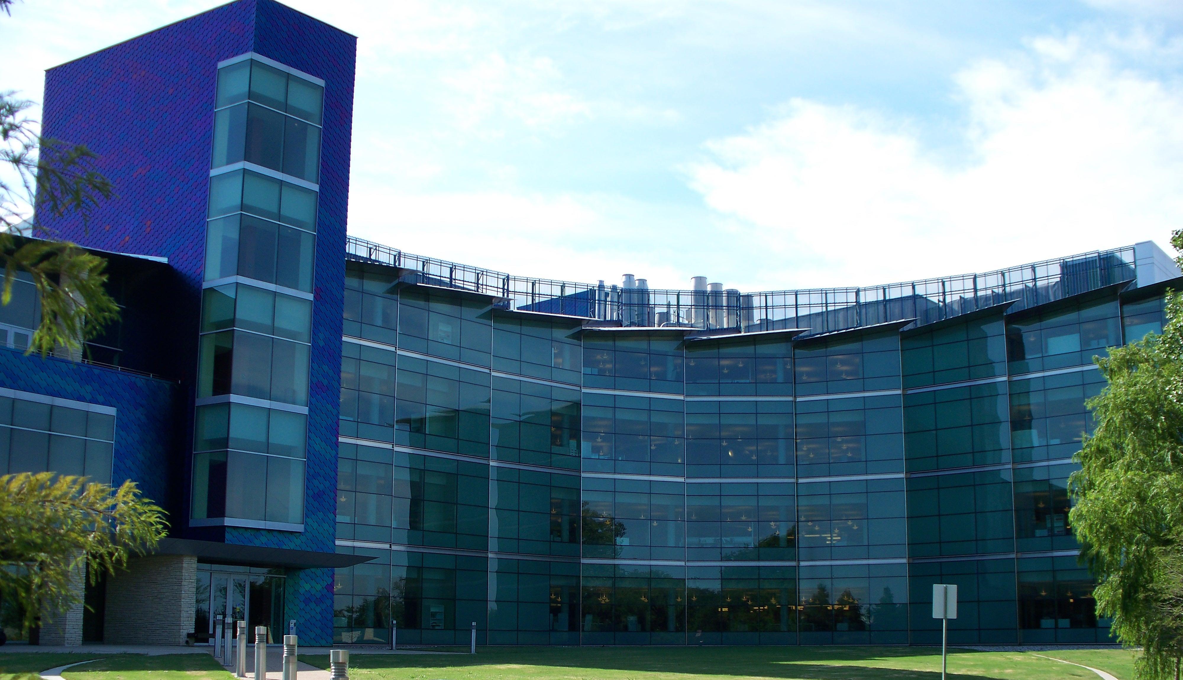
 Flexible and
Large Area Nanoelectronics
Flexible and
Large Area Nanoelectronics
Nano
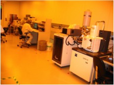
Characterization Facility
Atomic resolution TEM/STEM (JEM-ARM200F)
High resolution Analytical TEM/STEM with remote microscopy (JEM-2100F)
Dual column FIB/FEG SEM (FEI) with nano-manipulator, EDS, Cryo-transfer
E-beam litho (Zeiss Supra 40) with nano-manipulator, EBSD, EDS
Cryo, STM-TEM, AFM-TEM nano-factory, Heating, 3D tomography
Comprehensive Sample Preparation Lab.
Rigaku XRD: Ultima-III thin film system & Rapid Spider system
Scanning probe microscope (Veeco MultiMode V)
XPS, AES
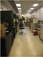
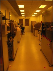
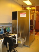
Our Facilities
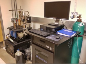
Hall system and
CCR
The Lake Shore 8400 Series can be used with both DC and AC field Hall
measurement methodologies to facilitate the broadest range of research
applications. The system includes fully integrated instrumentation, a
magnet and power supply, plus software that dramatically helps you
increase your research productivity and provides results that you can
trust. The system is capable of DC field measurements and has a
resistance range from 0.5 mΩ to 200GΩ. Measure Hall voltage, Hall
coefficient, Hall mobility, and resistivity. You can also determine
carrier density and carrier mobility versus temperature. For
temperature-dependent applications, the 8400 Series options enable you
to measure samples from 10 K to 350 K with a closed-cycle refrigerator
or take dedicated 77 K measurements with an optional single-point LN2
body.
Solar Cell
Characterization
For solar cell characterization we use a solar light source from
Newport (67005 Arc Lamp Housing), with its power source model
69907. These 67005 Arc Lamp Housing was designed for 50 to 500
Watt Hg, Xe and Hg(Xe) DC arc lamps. It uses a F/1 Single Element Fused
Silica condenser for a 1.3 inch (33 mm) diameter collimated beam at the
1.5 Inch Series output flange. For electrical measurement we use a
Keithley 2400 Source Measure Unit (SMU). This instrument is designed
specifically for test applications that demand tightly coupled sourcing
and measurement and can measure up to 200V, 1A and 20W.The power source
characteristics include low noise, precision, and readback. These
instruments can act as a voltage source, a current source, a voltage
meter, a current meter, and an ohmmeter.
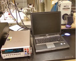
Electrical
Characterization
For
electrical characterization of materials, we
use Keithley 4200-SCS,
this tool is a modular, fully integrated parameter analyzer that
performs electrical characterization of materials, semiconductor
devices and processes. From basic I-V and C-V measurement sweeps to
advanced ultra-fast pulsed I-V, waveform capture, and transient I-V
measurements, the 4200-SCS provides the researcher or engineer with
critical parameters needed for design, development or production. For
C-V measurement, HP 4284A precision LCR meter is used. The wide 20 Hz
to 1 MHz test frequency range and superior test-signal performance
allow the HP 4284A to test components to the most commonly-used test
standards. These tools are complemented with a Cascade Microtech probe
station, with a Temptronics heated chuck which range from -25°C to
250°C to perform measurements at different samples temperatures.
Omnijet
100 Inkjet Printer, manufactured by Unijet (S. Korea)
Inkjet
printing is considered one of the most
popular methods for
solution-based deposition and noncontact patterning of organic
materials. The popularity of this method lies in its cost-effectiveness
and large-areas compatibility compared with other deposition techniques
that require high temperature and vacuum system. Inkjet printing
minimizes wastage of materials when fabricating devices; in most cases,
the volume of material that is needed is in the range of a few
picoliters (pL).
It
can be used to print materials on flexible, glass, Si or any other
substrate using various types of special inks, ranging from metal
nanoparticles to organic compound solutions. With the option of using
two types of cartridges, namely FujiFilm Dimatix and Samsung
cartridges. Can be loaded up to 4 different cartridges at a time with
different inks to print multi-structured complex circuits and devices.
The printer also has the capacity of heating the substrate when needed.
Features:
•
Four Refillable and cleanable cartridges (6 ml) in
one head module.
•
FujiFilm Dimatix and Samsung cartridge can be used.
•
Six automatic Motion stages with ± 7 ㎛ Stage
accuracy.
•
Auto Alignment with
automatic head rotation.
•
Single Droplet Measurement.
•
XY Servo Motor Stage, ± 5 ㎛
Repeatability.
•
300 x 210 mm effective
stroke.
•
Automatic Head & Work
Holder Rotation.
•
Heating substrate (20-150
°C).
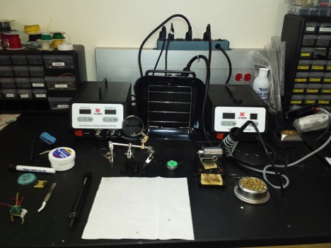
Soldering
Station
Our
soldering station is composed of two main
systems, the first one is
a Soldering/Desoldering Station LF-8800, a versatile tool able to
transfer temperatures from 300 to 896°F to its three components (Solder
Iron, Tweezers and Hot-Air Pencil), and the second one is a SMD Rework
Station LF-852D able to transferring heat from 212 to 896 °F through an
air flow (1.5L-40L/Min.) for mounting or dismounting electrical
components.
Both
with high accuracy for those kind of
simple/complex works that
need high precision like Surface-mount device (SMD) in which the
components are mounted or placed directly onto the surface of printed
circuit boards (PCBs). Being the Soldering Station the last step
(assembly) of our manufacturing process of electronic devices,
complemented by design / simulation / fabrication at laboratory-level
of electronic components (transistors, Diodes and Capacitors) and
design / simulation / fabrication of electronic boards.
ATC Orion-8
The
ATC Orion-8 sputter deposition system, by AJA International,
has the capability to co-sputter conductive and insulating materials on
substrates up to 4" in diameter. In addition to Ar sputtering, O2 is
also available for use in reactive-ion sputtering. The tool is equipped
with 2 RF (300W) and 1 DC (750W) magnetron sources. The substrate is
capable of heating to 850C while under rotation as well as exposure to
reactive gas and RF bias (50W). A cooled chevron prevents sputtered
material from entering into the turbopump. Software for control is also
available for automated film stack deposition.
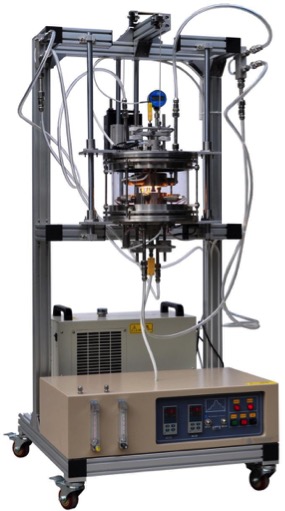
Closed Space
Sublimation
The
OTF-1200X-RTP-II is a two heating zone rapid
thermal processing
vertical tube furnace with 11" I.D. processing quartz tube and vacuum
flange. It is designed for PVD or CSS (Close Spaced Sublimation) film
coating up to 3" diameter or 2"x2"square. The furnace is heated by two
group halogen heaters (Top and Bottom) separately with max. 20şC/s
heating rate. Two 30 segment precision temperature controllers are
built in with +/-1şC accuracy. RS485 port and control software are
included to allow for operation of furnace and monitoring temperature
profile via PC.
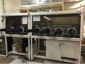
Gloveboxes
Our
Gloveboxes provide a clean, low-humidity,
Oxygen free environment
for laboratory, cleanroom, electronic assembly and other critical
processing operations in such industries as semiconductor
manufacturing. These Gloveboxes set up for Positive pressure operations
and when utilized with automatic purge control units, they can maintain
a preset relative humidity or oxygen level using an inert gas such as
Nitrogen.
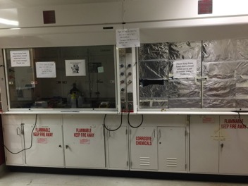
Hoods
Our hoods protect the user from harmful or toxic fumes or vapors
generated from a broad range of applications.
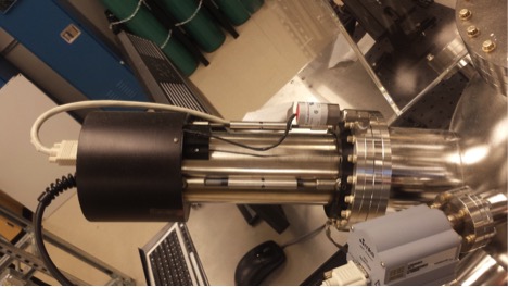
Pulsed Laser Deposition (PLD)
system
Pulsed
Laser deposition (PLD) is a versatile
thin film deposition technique. A pulsed laser rapidly evaporates a
target material forming a thin film that retains target composition.
The uniqueness of PLD is that the energy source (pulsed laser) is
outside the deposition chamber. This facilitates a large dynamic range
of operating pressures (10-7 Torr to 100 Torr) during material
synthesis. By controlling the deposition pressure and temperature, a
variety of nanostructures and nanoparticles can be synthetized with
unique functionalities. In addition, PLD is “digital” technique and
provides process control (Ĺ/pulse) at the nanoscale.
Our
lab count with two chambers, and we used
them for different purposes, which are described as follows:
a)
General purposes, where it is possible to deposit
a wide variety of chalcogenides, even transition metal di-chalcogenides
b)
Metal oxides such as ZnO,
In2O3, Ga2O3, IGZO,
HfO2, ITO, AZO, Al2O3, TiO2, among others.
The
system is available with a 248nm KrF excimer laser, where the frequency
of the shoots can be changed from 0.1 Hz to 25 Hz. The Lenses system
allow us to change the energy density from 0.1 J/cm2 to 2 J/cm2. It is
possible to deposit up to 3” substrate from RT to 850 °C. The maximum
number of targets allows at the same time is 6 of 1” of diameter and up
to 3 with 2” of diameter. Hence, Pulsed Laser deposition with
continuous composition spread is possible, this allows for a very rapid
successive deposition of each constituent at a rate of much less than a
monolayer per cycle, resulting in an approach that us fundamentally
equivalent to a co-deposition method. The fact that this method does
not depend on a post-deposition anneal to promote interdiffusion or
crystallization makes it applicable to studies where growth temperature
is critical parameter, or to situations where high temperatures anneals
are incompatible with either the deposited material or substrate.
Pulsed Electron
Deposition
Our system is quite versatile, because Pulsed electron deposition is
possible. PED is a process in which a pulsed (100ns) high power
electron beam (approximately 1000 Ĺ, 15 keV) penetrates approximately 1
μm into the target resulting in a rapid evaporation of target material,
and its transformation in plasma state. The non-equilibrium
extraction
of the target material (ablation) facilitates stoichiometric
composition of the plasma. Under optimum conditions, the target
stoichiometry is thus preserved in the deposited film. All solid state
materials-metals, semiconductors and insulators, can be deposited as
thin films with PED. Unlike PLD where the ablation process is
critically dependent on the optical absorption coefficient of the
target material, in PED, the ablation depends only on the range of
electrons in the target.
DXR Raman microscope
Lateral
resolution (xy) up to 1 µm and depth resolution up to 2 µm, a spectral
range from below 100 to 3600 cm-1 with a spectral resolution up to 2
cm-1 one excitation lasers (532nm)