| THE PLASMA APPLICATIONS LABORATORY (PAL) |
 |
Photos of the Plasma Applications Laboratory.
 |
This is a photo of an inductive source for creating highly uniform high density plasmas. The multiple layers allow one to control the rf B-fields with better accuracy for higher uniformity. |
 |
This is a photo of an inductive source for creating highly uniform high density plasmas. Marwan Khater is holding this source since he and Larry Overzet designed it and have filed for a patent on it. |
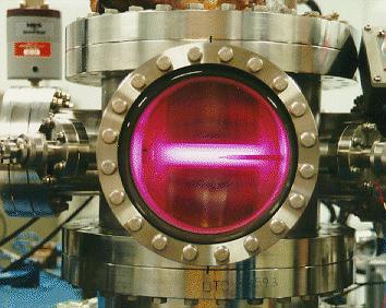 |
This is a photo of the GEC reactor with an argon plasma. The RF power is capacitively coupled to the glow in this instance, and so you can see the two electrodes used to excite the plasma at the top and bottom. The upper electrode is powered with RF while the lower electrode is grounded. The window in the front is circular and has an ID of about 6 inches. In the background at the upper left is the capacitance manometer used to measure the pressure. |
 |
This is a photo of an argon plasma in the GEC reactor as well. In this case it is a closer look at the plasma itself. Extending into the glow from the right hand side is a Langmuir probe we use to measure the plasma properties. The upper electrode is powered with RF (at 13.56 MHz) while the lower electrode is grounded. |
 |
This is a photo of the GEC reactor with an argon plasma. Siva is looking at the frequency components of the RF voltage and current on the computer screen. The computer updates the first 5 RF harmonics every 0.5 second or so. You can sort of see what the rf voltage (white trace in the upper left hand corner of the computer screen) and current (the red trace in the same place) look like. The plasma's glow is visible in the window of the chamber and several instruments for making measurements of the plasma are visible as well. |
 |
This is a photo of the Lab in which the GEC reactor is operated. It is one of the three lab spaces that make up the Plasma Applications Laboratory. As time permits, we will take pictures of the other two lab spaces as well. |
 |
This is a photo of a capacitively coupled discharge in a glass chamber. One nice thing about glass chambers is that they allow one to fully see the plasma. In this photo, one can easily see the glow region, the sheaths (or dark spaces) and the electrodes. The driven electrode is on the left hand side of the glow and has three parts. The thin metal stripe is the electrode itself, the white band is a teflon insulator and the metal at the left is a ground plane that prevents the glow from striking behind the electrode. On the right hand side is an inlet to an energy resolving mass spectrometer. |
 |
This is a photo of Chris making a Langmuir probe for use in the GEC reactor. He is soldering the internal components together at this point. Chris is an Engineer for Texas Instruments, Inc. |
 |
This is a photo of an ICP plasma through argon in the GEC reactor. While the plasma appears to be well confined in the picture, the elctron density extends well beyond the electrode radius. |
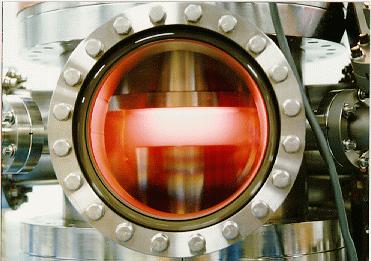 |
This is a photo of an ICP plasma through nitrogen in the GEC reactor. The nitrogen plasma can be significantly brighter than a comparable argon plasma. |
 |
This is a photo of the GEC reactor with a nitrogen plasma from further out. |
 |
This is a photo of the GEC reactor with a nitrogen plasma from further out as well. |
 |
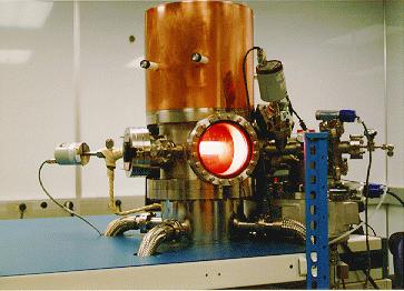
This is a photo of the PAC200 processing reactor which was donated by Texas Instruments Inc. It allows us to process up to 6 inch wafers. Marwan will be outfitting this reactor with an inductively coupled source during 1996. |
 |
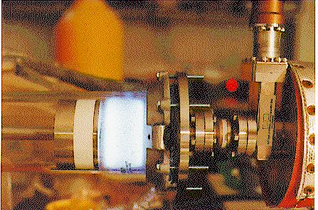
This is a photo of our helical resonator source and mass spectrometer. Brian has computer automated this setup so that we can obtain detailed mass and ion energy spectra of the plasmas we generate here. The plasma in this case is through SF_6. |
 |
 |
 |
 |
 |
 |
|
| Main Page | L.J.O. Vita | P.A. Lab | Presentations | Course Info. | Teaching On-Site | Consulting |
University of Texas at Dallas, P.O. Box 830688, EC33 Richardson, TX 75083-0688 Tel: (972)883-2154 Fax: (972)883-6839 email: overzet@utdallas.edu
Return to Department of Electrical Engineering Home Page