Heterostructures are able to improve the performance of semiconductor devices because they permit the device designer to locally modify the energy-band structure of the semiconductor and so control the motion of the charge carriers. In order to understand how such local modification of band structure can affect this motion, one needs to understand the energy bands of bulk semiconductors [13].
If a number of atoms of silicon, for example, are brought together
to form a crystal, the discrete energy levels of the free atoms broaden
into energy bands in the crystal. The reason for this is that the
electrons are free to move from one atom to another, and thus they can
have different amounts of kinetic energy, depending upon their motion.
Each of the quantum states of the free atom gives rise to one energy
band. The bonding combinations of states that were occupied by the
valence electrons in the
atom become the valence bands of the crystal. The anti-bonding combinations
of these states become the conduction bands. The form of the wavefunctions
of band electrons is specified by the Bloch theorem to be of the form
 ,
where n labels the energy band,
,
where n labels the energy band,  is the wavevector of the state, and
 is a periodic function on the crystal lattice.
Each such state has a unique energy
is a periodic function on the crystal lattice.
Each such state has a unique energy  , and a plot of
this energy as a function of
, and a plot of
this energy as a function of  represents the energy band structure.
For most purposes we can confine the values of
represents the energy band structure.
For most purposes we can confine the values of  to lie within a solid
figure called the Brillouin zone. Perspective plots of the energy band structures
derived from an empirical pseudopotential model [14]
for Si and GaAs are plotted in
Figures 1 and 2, respectively.
to lie within a solid
figure called the Brillouin zone. Perspective plots of the energy band structures
derived from an empirical pseudopotential model [14]
for Si and GaAs are plotted in
Figures 1 and 2, respectively.
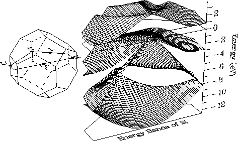
Figure 1: Perspective plot of the energy band structure of silicon.
The figure to the left shows the Brillouin zone, and the two-dimensional section
over which the energy bands are displayed. The energy bands are plotted to the
right. The four surfaces lying below 0 eV are the valence bands, and the upper
 , which on this figure is the center of the front boundary of the
Brillouin-zone section.
The minimum conduction-band energy occurs
along the front boundary of the section, near the left and right ends. Thus,
Si has an indirect-gap band structure.
, which on this figure is the center of the front boundary of the
Brillouin-zone section.
The minimum conduction-band energy occurs
along the front boundary of the section, near the left and right ends. Thus,
Si has an indirect-gap band structure.
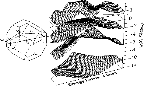
Figure 2: Perspective plot of the energy band structure of gallium
arsenide. The conventions of the figure are the same as those of Fig. 1.
The conduction-band minimum of GaAs occurs at  , and thus GaAs has a
direct-gap band structure.
, and thus GaAs has a
direct-gap band structure.
The dynamics of electrons in energy bands are described by two theorems [13].
The velocity of an electron with wavevector  is given by the group velocity:

If a constant force  is applied to an electron, its wavevector will change
according to
is applied to an electron, its wavevector will change
according to

If the band structure is perfectly parabolic,  , these reduce to the
ordinary Newtonian expressions. However, as shown in Figs. 1 and
2, there are large regions in the band structures of ordinary
semiconductors were they are not parabolic.
, these reduce to the
ordinary Newtonian expressions. However, as shown in Figs. 1 and
2, there are large regions in the band structures of ordinary
semiconductors were they are not parabolic.