The central feature of a heterojunction is that the bandgaps of the participating semiconductors are usually different. Thus, the energy of the carriers at at least one of the band edges must change as those carriers pass through the heterojunction. Most often, there will be discontinuities in both the conduction and valence band. These discontinuities are the origin of most of the useful properties of heterojunctions.
As with all semiconductor
devices, the key to understanding the behavior of heterojunctions
is the energy-band profile which graphs the energy of the conduction and valence
band edges versus position. The position-dependent band-edge energies are just
the total potential appearing in (3), and we will use the
symbols  and
and  to
denote these quantities for the conduction and valence bands, respectively. Thus,
to
denote these quantities for the conduction and valence bands, respectively. Thus,
In a heterojunction, the dependence of  and
and  upon x are due
to the combined effects of the electrostatic potential
upon x are due
to the combined effects of the electrostatic potential  and the
energy-band discontinuities or shifts due to the heterostructure. In
the earlier literature on heterojunctions, this latter effect is usually
described in terms of the electron affinity
and the
energy-band discontinuities or shifts due to the heterostructure. In
the earlier literature on heterojunctions, this latter effect is usually
described in terms of the electron affinity  [18,10].
However, the electron
affinity model is not a very accurate description of
heterojunctions [19],
so we will simply view the band-edge energies
[18,10].
However, the electron
affinity model is not a very accurate description of
heterojunctions [19],
so we will simply view the band-edge energies  as fundamental properties of the
semiconductors participating in the heterostructure. Thus, in a heterostructure,
as fundamental properties of the
semiconductors participating in the heterostructure. Thus, in a heterostructure,
 appears in the effective-mass Schrödinger equation (3)
as a function of position. [The effective mass
appears in the effective-mass Schrödinger equation (3)
as a function of position. [The effective mass  is also a function of
position, but the Hermitian form of (3) accounts for its variation.]
The question of what is the appropriate reference energy for
is also a function of
position, but the Hermitian form of (3) accounts for its variation.]
The question of what is the appropriate reference energy for  to permit a comparison
of different semiconductors is the key question in the theory of the heterojunction
band alignment.
To begin our investigation of the band alignment, let us assume that
the structure has been so designed that each semiconductor is precisely
charge-neutral, and thus
to permit a comparison
of different semiconductors is the key question in the theory of the heterojunction
band alignment.
To begin our investigation of the band alignment, let us assume that
the structure has been so designed that each semiconductor is precisely
charge-neutral, and thus  will be constant and may be neglected.
In such circumstances, we may focus upon the behavior of
will be constant and may be neglected.
In such circumstances, we may focus upon the behavior of  and
and
 in the vicinity of the heterojunction.
It has been found experimentally that there is no a priori relation between the band-edge energies of the two semiconductors forming a heterojunction, despite theoretical proposals of universal band alignments by Adams and Nussbaum [20] and by von Roos [21]. (These proposal were critiqued by Kroemer [22].) We therefore need a general scheme within which heterojunction band alignments may be described. The quantities used to describe the band alignment are defined in Fig. 3.
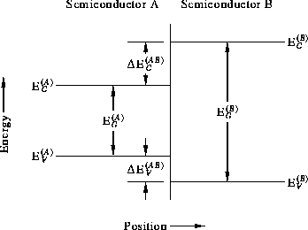
Figure 3: Definition of the quantities required to describe the
band alignment of a heterojunction.
The one quantity which is known with great certainty is the total bandgap discontinuity,

where  and
and  are the energy gaps of
materials A and B, respectively. The total discontinuity is
divided between the valence and conduction band discontinuities,
defined by
are the energy gaps of
materials A and B, respectively. The total discontinuity is
divided between the valence and conduction band discontinuities,
defined by
Clearly, the individual discontinuities must add up to the total discontinuity,

How the discontinuities are distributed between the valence and conduction bands is the major question to be answered by theory and experiment.
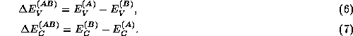
To illustrate the diversity of band alignments available, Figures 4--10 illustrate the best estimate of the band alignment for seven lattice-matched heterojunctions between group III-V semiconductors, from a tabulation by Yu and co-workers [23]. Energies are indicated in electron Volts.
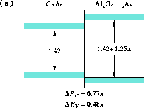
Figure 4: Band alignment of GaAs-Al Ga
Ga As in the direct-gap range.
Figure 5: Band alignment of In Ga
Ga As-InP
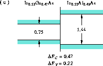
Figure 6: Band alignment of In Ga
Ga As-In
As-In Al
Al A.
A.
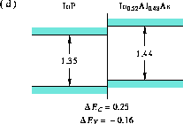
Figure 7: Band alignment of InP-In Al
Al As
As
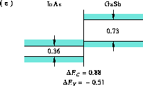
Figure 8: Band alignment of InAs-GaSb
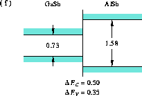
Figure 9: Band alignment of GaSb-AlSb
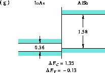
Figure 10: Band alignment of InAs-AlSb.
Shown are the band alignments of
(a) GaAs-Al Ga
Ga As in the direct-gap range [23],
(b) In
As in the direct-gap range [23],
(b) In Ga
Ga As-InP [24],
(c) In
As-InP [24],
(c) In Ga
Ga As-In
As-In Al
Al As [24],
(d) InP-In
As [24],
(d) InP-In Al
Al As [25],
(e) InAs-GaSb [26],
(f) GaSb-AlSb [27], and
(g) InAs-AlSb [28].
The topology of
the band alignments are classified according to the relative ordering of the
band-edge energies [29]. The most common (and generally
considered to be the ``normal') alignment is the straddling configuration illustrated
in Figures 4, 5, 6, and 9.
The bandgaps
need not entirely overlap, however. The conduction band of the smaller-gap
material might lie above that of the larger-gap material, or its valence
band might lie below that of the larger-gap material. Such a band alignment
is called staggered, and is known to occur in the
In
As [25],
(e) InAs-GaSb [26],
(f) GaSb-AlSb [27], and
(g) InAs-AlSb [28].
The topology of
the band alignments are classified according to the relative ordering of the
band-edge energies [29]. The most common (and generally
considered to be the ``normal') alignment is the straddling configuration illustrated
in Figures 4, 5, 6, and 9.
The bandgaps
need not entirely overlap, however. The conduction band of the smaller-gap
material might lie above that of the larger-gap material, or its valence
band might lie below that of the larger-gap material. Such a band alignment
is called staggered, and is known to occur in the
In Ga
Ga As-GaAs
 Sb
Sb system [26], as well as those of
Figures 7 and 10.
The staggering might become so extreme that the bandgaps cease to overlap.
This situation is known as a broken gap, and such a band
alignment is observed in the GaSb-InAs system, Figure 8.
Another nomenclature
is occasionally employed, usually in describing superlattices, which
are periodic heterostructures. If the extrema of both the
conduction and valence bands lie in the same layers, the
superlattice is referred to as ``Type I,'' whereas if the band
extrema are found in different layers the superlattice is ``Type
II.'' Aside from being rather uninformative, this notation makes
no distinction between the staggered and broken-gap cases, and
the more complete nomenclature described above should be
preferred.
system [26], as well as those of
Figures 7 and 10.
The staggering might become so extreme that the bandgaps cease to overlap.
This situation is known as a broken gap, and such a band
alignment is observed in the GaSb-InAs system, Figure 8.
Another nomenclature
is occasionally employed, usually in describing superlattices, which
are periodic heterostructures. If the extrema of both the
conduction and valence bands lie in the same layers, the
superlattice is referred to as ``Type I,'' whereas if the band
extrema are found in different layers the superlattice is ``Type
II.'' Aside from being rather uninformative, this notation makes
no distinction between the staggered and broken-gap cases, and
the more complete nomenclature described above should be
preferred.
