130nm Process - IBM130 Technology
0. Setup Environment
This step will add correct PATH to your shell and take effect. You don't need to setup PATH afterwards. only need run once.
echo 'export PATH=$PATH:/bin' >> ~/.bashrc && exec $SHELL -i
You will need to make a working directory. To do this, type the following command in your home directory in the terminal:
/proj/cad/startup/setup-ibm130-cad
This will automatically create a directory named cad. Now go to this directory and list its contents by typing:
cd cad
ls -a
You will see five directories for different purposes:
cadence         : Cadence
siliconsmart    : Library Characterization
primetime       : Static Timing Analysis
se              : Auto Place & Route (Encounter)
synopsys        : Verilog HDL Synthesis
spice           : Hspice Simulation
You should do the different projects in their respective directories. For example, do all cadence work in the cadence directory, Siliconsmart library characterization in siliconsmart directory, etc. These tools create a lot of files. By separating their workspaces, you will avoid confusion amongst the files.
Now go to the synopsys directory and list its contents:
cd synopsys
ls -a
You should see only one file - .synopsys_dc.setup. Now go back to where you were:
cd ..
Now go to the cadence directory and list its contents:
cd cadence
ls -a
You will see two directories: Assura and Spectre; and five files: .cdsenv, .cdsinit, display.drf, cds.lib and assura_tech.lib.
Now go back to where you were:
cd ..
Now do the same for the other directories that you did for synopsys and cadence. This completes your tour of working directories.
In the future when you do any cadence work, you will need to go to the cadence working directory:
cd ~/cad/cadence
Same for siliconsmart, primetime, synopsys, se and spice:
cd ~/cad/siliconsmart
cd ~/cad/primetime
cd ~/cad/synopsys
cd ~/cad/se
cd ~/cad/spice
Source Profile
Each time you open a shell (new terminal) to start any of cad tools, you need to source the corresponding links always.
For Cadence tools (Cadence, Encounter):
. /proj/cad/startup/profile.ic-5
The Assura DRC/LVS/QRC are only available on engnx servers.
For Synopsys tools (Library Compiler, Design Vision, Hspice, Primetime, etc.):
. /proj/cad/startup/profile.synopsys_2018
Note
1.Without sourcing the proper link, the cad tools will NOT work.
2.If you intend to use both Cadence tools and Synopsys tools, use them in different terminals (sessions), e.g. use icfb in one terminal, and use Hspice in another, after sourcing proper profiles.
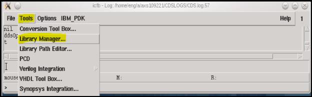
1. Start Cadence
Go to cad/cadence folder by entering this command:
cd ~/cad/cadence
Setup your environment by sourcing the proper profile.
. /proj/cad/startup/profile.ic-5
If you went through the setup section, you should have the library file and display files for cadence (two directories: Assura and Spectre; and five files: .cdsenv, .cdsinit, display.drf, cds.lib and assura_tech.lib). If you haven't setup since then, please do so.
There are several ways to start Cadence depending on which features are needed. We will use icfb.
Start Cadence by:
icfb &
This will start Cadence and open the Library Manager window. Through the Library Manager you can manage your design process and use various Cadence features. This window shows reference libraries including analogLib, cdsDefTechLib, basic, esd8rf, and cmrf8sf. Make sure that all of these libraries show in the Library Manager window. You will use analogLib for building schematic views. cmrf8sf is the technology library for the IBM130 CMOS Process Technology.
Quit Cadence
To quit Cadence, select File -> Exit from the Library Manager pull-down menu.
A message window appears to confirm. Select OK to exit.
For more information regarding Cadence, refer to the online manual through the Help pull-down menu in the Library Manager, or access it from the command prompt by typing opsenbook.
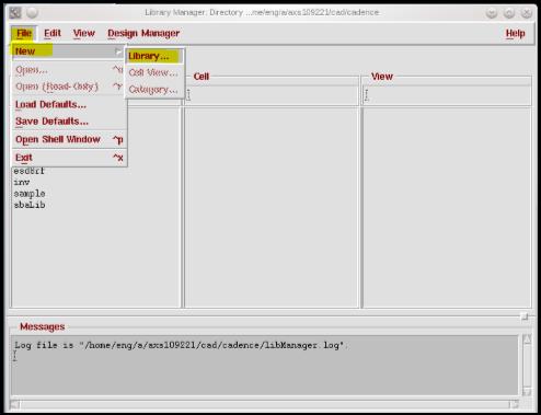
2. Create Design Library
The first step of IC design in Cadence is to create a design library so you can develop your design. Design libraries are the places where you store your designs.
Now we are going to create a design library named tutorial.
-
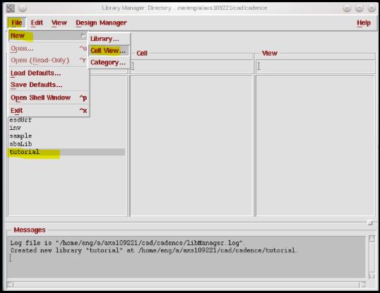
On the icfb window choose Tools -> Library Manager
-
In the Library Manager Click on File -> New -> Library..
-
Type tutorial or any library name you want.
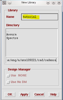
-
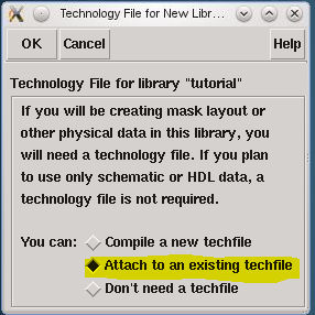
Click on OK. Then chose the option of Attach to an existing techfile
-
Choose cmrf8sf and hit OK.
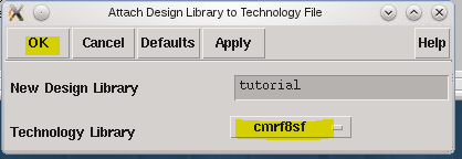
The technology file is then compiled and the library is created. You can see tutorial appears in Library Manager Window. Click tutorial to see what do you have in it. Of course, there's nothing there at this moment. You can check on cmrf8sf too. It contains standard cells symbolic cells defined in the technology. You can click left on cells to see what views do they have.
3. Creating Different Cell Views
Once you have created a design library, you can start to put your design into it. We are going to design a inverter (INV) as example
3.1 Create Layout view
-
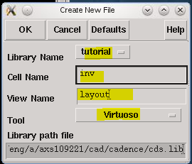
Next make sure tutorial is highlighted in the Library Manager window, it means click tutorial first then click on File -> New -> Cell View..
-
Since you are going to draw the layout of inverter choose Virtuoso under Tool
Now you can start drawing the layout!
In Library Manager window, click left on tutorial library. You will see the tutorial library inv cell, and layout cellview high-lighted. Then in Library Manager pull down menu, select File -> Open
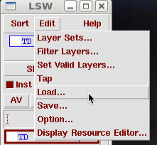
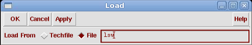
Load lsw
ON LSW window, you must have tons of layers there. Go to Edit -> Load
On your Load window, check File, and fill lsw in the blank, then press OK. You will see the only layers that you need to use for this class.
If you want to diable some more layer, go to LSW -> Edit -> Set Valid Layer find layer and uncheck, or check if you want to enable.
Drawing a rectangle
The most common shape in a layout is rectangle. To draw rectangles
- From LSW select a layer by clicking left mouse button on it. You will see the selected layer surrounded by wider border (the selected layer is hightlighted).
-
From Virtuoso Layout Editing window pull down menu, select Create -> Rectangle
-
In the layout design window (Virtuoso Layout Editing) click left mouse button for the first corner of the rectangle, then click left mouse button again for the second corner. A rectangle is drawn.
- If this is not the desired rectangle, select Edit -> Undo from menu to undo the action.
- If you want to draw another rectangle using current drawing layer, simply click left mouse button for the two corners of the rectangle.
- If you want to draw rectangles of another layer, click left mouse button to select your layer in LSW to change the drawing layer then click left mouse button for the two corners in Virtuoso Layout Editing window.
- If you have finished drawing rectangles, hit Esc on the key board to exit from
Create Rectanglecommand. - Please make sure that your snap spacing is 0.01 for both X snap spacing AND Y snap spacing. You can check by doing the following: Click Options -> Display.
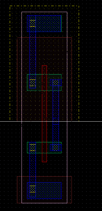
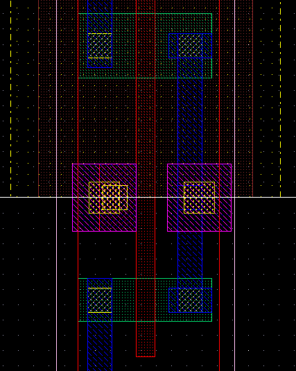
Inverter Layout Tutorial
-
Click on NW drw (N-well) in the layers window that pops up and create a rectangle which looks like the picture shown below. Do not worry about sizing for now this is just a tutorial however you need to worry about the sizes for the actual layout.
-
Click on RX drw (diffusion) and create four rectangles as shown. Two of the rectangles will reside in the NW, and the other two will be outside the NW.
-
Click on GRLOGIC drw and create a rectangle that covers all four rectangles as shown below.
-
Next click on prBoundary drw and create a rectangle on top of GRLOGIC drw you just draw. This is the Place and Route boundary to your cell. If you can't find prBoundary in LSW window, you need to load lsw.
-
Click on BP drw and create a rectangle that covers the second RX rectangle and another BP drw rectangle that covers the forth RX rectagle as shown below.
-
Click on PC drw (poly) and create a bar that crosses the middle two RX rectangles as shown.
Now the next step is to put in the contacts that connect each component.
Putting Contacts
-
Click on CA drw (contact) and place rectangles of the size 0.16u x 0.16u in the places shown below.
-
Click on M1 drw (metal 1) and draw rectangles that cover the CA drw rectangles drawn previously as shown in the picture.
-
Using the same M1 drw layer, draw two rectangles that covers the first and fourth RX drw rectangles.
-
Click on PC drw (Poly) and create a rectangle as shown in the picture.
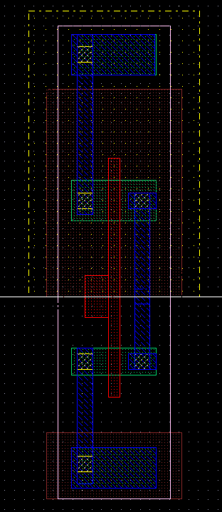
-
Click on CA drw and place it on the POLY rectangle created in the previous step as shown below. Then, click on M1 drw and create a rectangle that goes on top of the PC rectangle. Make sure that the M1 rectangles are at least of size 0.089um^2.
-
Click on M2 drw (metal 2) and create a rectangle of at least size 0.120 um^2 and put it on top of the METAL1 rectangle created in the previous step. Now click on V1 drw and create rectangle of size 0.2u x 0.2u and put it in the middle of the two rectangles just created.
-
Do the same for the right side as shown below: Create rectangles using M1 drw and M2 drw and overlap them. Then create a rectangle using V1 drw (Via 1) and put it in the middle of the rectangles.
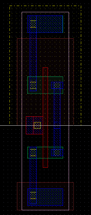
Now what is left is creating pins of inputs and outputs.
Putting Pins
Pins define where the wires outside the cell can be connected to the cell. In our case, we need pins for in, out, vdd and ground. To create all of these pins
DON'T USE ANY UPPER CASE NAMES FOR YOUR PINS AND CELL NAMES
-
Click on M1 pn.
-
From Virtuoso pulldown menu, select Create -> Pin... . This brings out
Create Symbolic Pinwindow. Select shape pin in Mode field, thenCreate Shape Pinwindow comes out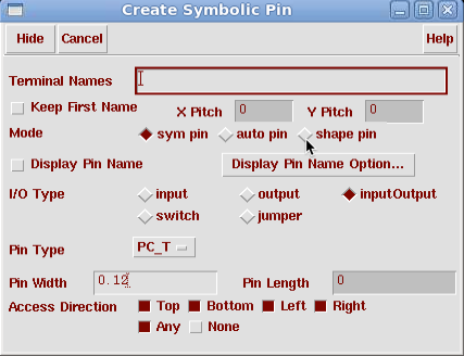
-
Fill in vdd! and gnd! in
Terminal Names. Make sure mode is rectangle, theDisplay Pin Nameis checked andIO typeis inputOutput. Also make sureAccess Directionis left and right ONLY.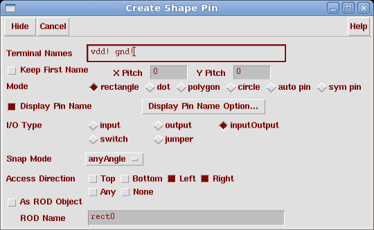
-
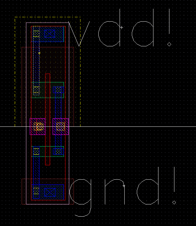
Create rectangles in the first and fourth rectangles as shown below by creating a rectangle in the first rectangle then in the fourth.
-
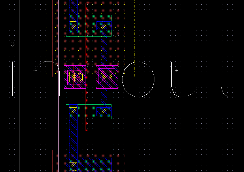
Now you will create the input pin named in. In LSW, select M2 pn pin layer. It is the metal2 layer with pin purpose. In
Create Shape Pinwindow select input asI/O typeand select top and bottom asAccess Direction(you might need to unselect left and right). Create a rectangle in the left POLY rectangle as shown below.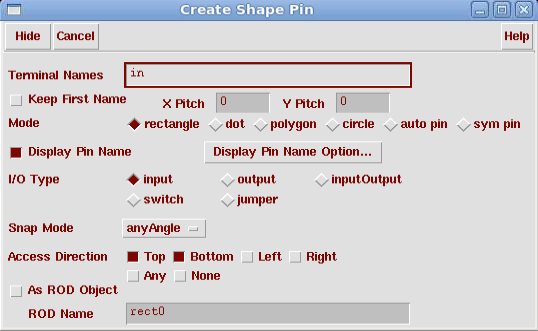
-
The next pin is output named out. Similar as input pin of previous step, but select output as
I/O type. Creat a reactangle in the METAL1 & METAL2 overlap on the right as shown below.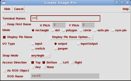
Layout Tips
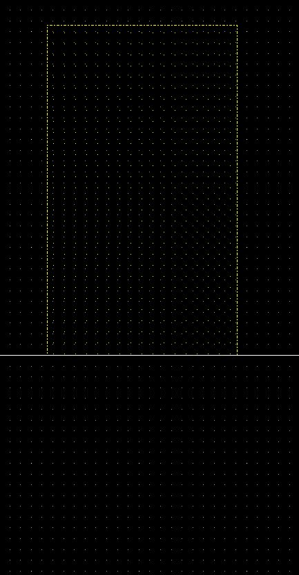
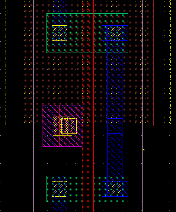
1) Pin pitch and offset
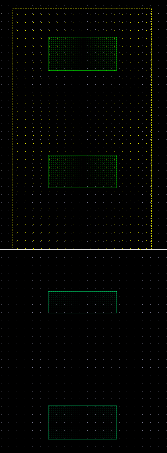
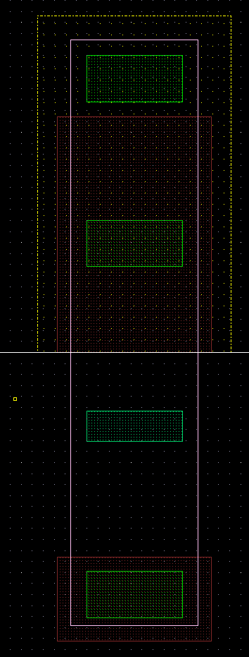
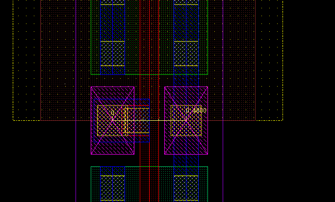
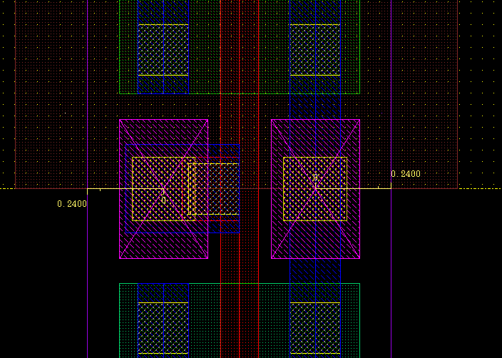
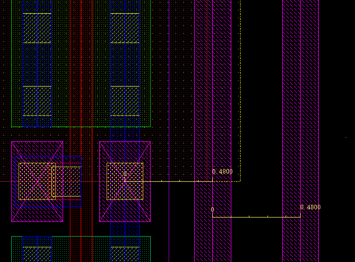
For our project design, in the cell library design, the distance between pins should be 0.48*n (n=1, 2, 3...) um. And the distance between the GRLogic and its adjacent pin should be 0.24+0.48*n (n=0, 1, 2, 3...) um. The reason is that when we use encounter to assign the layout automatically, the cells will bond by prbond layer, which here is the same figure as the GRLogic. A distance of 0.24+0.48*n in one cell will make the first adjacent pins between two bonded cells have a distance 0.48*m (m=1, 2, 3...). Fig. 1 and 2 show the example.
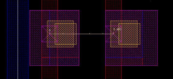
Figure 1. Distance between pins, here it is 0.48um
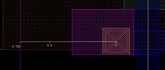
Figure 2. Distance between the bond and the first pin, here it is 0.24+0.48 um; the blue line on the left is prbound, it overlap exactly the GRLogic, that means in our project design we can draw prbound and GRLogic the same.
The smallest distance between the boundary and the first pin would be 0.24um.
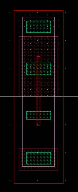
2) GRLogic
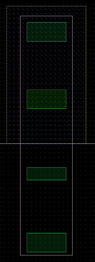
When drawing the GRLogic, the upper and lower bond should match the upper and lower M1 bonds. That will void the auto layout misalignment in the encounter process. Figure 3 shows an example.
Also, make your vdd/gnd rails as wide as the GRLogic, so that when the cells are placed side by side in the future layout tools, the vdd/gnd of neighbouring cells will be touching each other automatically.
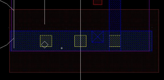
Figure 3. The lower bond of prboundary matches the lower bond of M1 exactly
3) prBoundary
The prboundary is the actual bond by which different cells connect in the encounter process. The GRLogic is not that critical. But we can draw the GRLogic the same as the potential prbond in the first place; and then draw a same prbound in the last step.
4) Layer dimensions and distances
Length of poly is 0.12um;
Distance between two RXs is 0.6um (Vertical);
Distance between two ploys is 0.2um;
Distance between two contacts is 0.24um;
Distance between two M1 is 0.16um;
Distance between RX and contact is 0.06 um;
Distance between two V1 is 0.28um
Width of M1 is 0.16um;
Width of M2 is 0.2um;
Distance between RX and contact (Horizontal) is 0.1 um;
Length of V1 square is 0.2 um;
Length of contact square is 0.16 um;
Contact is used to bond diffusion and M1, or poly and M1. The M1 to M1 connection needs no contact. V1 is used for connecting M1 and M2. There is no cross for the same metal, or it will give a short circuit.
Pins are supposed to be in the same track (same size and same y-coordinate); otherwise in the encounter process the there will be warning on off grid.
5) DRC/LVS/QRC
DRC is to check whether the layout drawing match the design rules in the system, based on the IBM 130nm technology. LVS is to check whether your schematic and layout match well. RCX/QRC is to generate the spice netlist based on LVS;
6) Cell sizes
The cell size is the GRLogic size. The height should start from the bottom of GND M1 to the top of VDD M1.
Your VDD/GND should extend to be the same width of GRLogic.
The cell library is all the cells you design for the final system automatic layout by encounter. Try to make all the cells with same height. That means they should have same prbond (GRLogic) height, with no relation to NW or BP. You can choose different NW and BP height for different cells, but to make sure that they are big enough.
7) Before drawing the D Flip-flop layout, try to find out the minimum number of Euler Trails, as professor taught in the class.
8) Create pins
When you draw the pins, you may want to show the pin names. Here is an instruction for the correct process:
- Choose the pin layer (M1 pn, M2 pn, etc.) you wan to draw in the LSW;
- Choose the Drawing Rectangle shape in the left tool bar;
- Go to Create -> Pin, configure the pin options;
Then you can draw the pin as you want. Please be advised that this sequence is kind of strict. If you put 3 before 2 you will get a pin without pin names display. That is a problem many students met in the design.
9) Prboundary
In the Abstract View Establishment step, if you can not get a prbound from the Auto Boundary, you need to draw the prBound by yourself. Normally there is not a prBound in your LSW so you need validate it by yourself by setting it in the LSW. Then when you draw the prBound, you can exactly make it like your GRLogic. Regarding the design tips for GRLogic and prBound you can check them from 2).
10) Inverter layout
In the Inverter design (Proj. 3), if you are a total new student for VLSI design, I think you may feel completely confused by those different shape and drawing. As below is a brief explanation for that.
- In this inverter design the instruction does not ask for any size requirement. And it doesn't give any size details. But actually we need to choose minimum size, which means minimum height and width for the whole inverter. Since this design is just to let you be familiar with the layout design, there is no size requirement, but we should know this point.
- If you want to choose the minimum size, which means all sizes requirement should meet the data in 4). An example is that the distance between two RXs is 0.6um. The length of the poly is 0.12um.
- Before you design the inverter, try to be familiar with the design rule of layout. Following the tutorial like a machine is not a good idea.
11) DO put all input and output pins in the same track, except vdd and gnd. If you put pins in different tracks, the automatic routing and placing will generate errors.
12) Layout shortcuts:
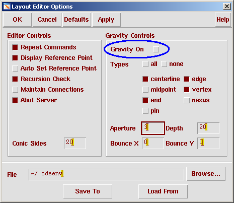
13) Virtuoso options setting
If you can't move your cursor freely in the layout window, go to Options -> Layout Editor, uncheck the Gravity On
Click OK.
Also go to Options -> Display, check Pin names to be able to see your pin names.
If you want to move your cursor freely instead of horizontally and vertically, change the Snap Modes into anyAngle.
14) About the cell library boundary distances
The distance between two V1 is 0.28um. So that requires that the V1 in your outside pins (closest to the boundary) must be 0.14um apart from the distance. Otherwise, you will get a lot of DRC error about the vias in your final layout after encounter.
Same rules apply to M1, M2, RX layers:
The distance between two M2 is 0.2um. M2 to boundary min distance is 0.1um.
The distance between two M1 is 0.16um. M1 to boundary min distance is 0.08um.
The distance between two RX is 0.18um. RX to boundary min distance is 0.09um (we would prefer 0.1um).
Design Rules
RX and PC
CA and M1
Cell Measurement
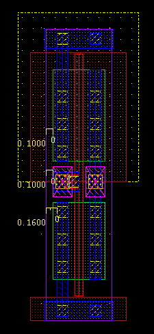
In order to use automatic placing and routing tools, we need to make sure all inputs and outputs of a cell is on the pitch size and the height of every cell in your library is the same. The height is determined by the largest cell your have (usually the flip-flop)
At this time, I believe you understand about pitch and grid of them. To measure the area of cells, you have to know your cell height and width.
The purple rectangular is the actual boundary of your cell. Any thing outside the cell boundary could overlap with other cells. For example, the n-well is outside the boundary but all cells have the same location for n-well. So, it is ok to let n-well, vdd, gnd extended a little bit and overlap with others.
Measuring Height is simple
Your height will be from bottom of your gnd rail to top of your vdd rail
Measuring Width can be a little bit more tricky
First, make sure your I/O pins ( M2 drw and M2 pin Layers, it is better if they are overlap with each other) on grid
I believe the minimum pitch size is 0.48 um. It can be bigger depending on your design.
For this example, Pitch size is 0.48 um (distance between two close possible I/O Pins)
Distance between pins can be (const) * pitch size
And you also have to have (const + 1/2) * pitch from pin to both side boundaries. This case const is 0, but it can be other constant number for complicated design like DFF.
You should also make sure that from the side boundaries,
- diffusion area has to be spaced at least 0.1um (because diffusion spacing distance is 0.2 um). If two cells placed next each other, the space has to be bigger than 0.2um
- Metal2 has to be spaced at least 0.1um (because M2 spacing distance is 0.2 um) If two cells placed next each other, the space has to be bigger than 0.2um
- Metal1 has to be spaced at least 0.08 um (because Met1 spacing distance is 0.16 um) If two cells placed next each other, the space has to be bigger than 0.16um
The distance between two V1 is 0.28um. V1 to boundary min distance is 0.14um.
The distance between two M2 is 0.2um. M2 to boundary min distance is 0.1um.
The distance between two M1 is 0.16um. M1 to boundary min distance is 0.08um.
The distance between two RX is 0.18um. RX to boundary min distance is 0.09um (we would prefer 0.1um).
And make sure other layers have correct spacing.
However, your N-well, BP, VDD rail, and GND rail need to be extended from the boundary, because they will be shared with other cells.
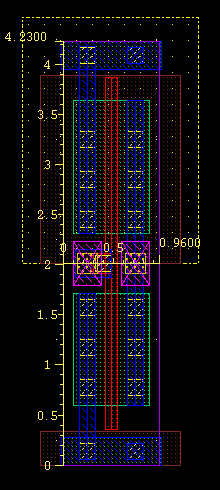
So, the area of this cell is
Height = 4.23 um
Width = 2 pitch size ( your width is always (const)* pitch size) = 2 * 0.48 um = 0.96 um
Area = 4.23 * 0.96 = 4.06 um^2
If you are using Metal2 in cell block, make sure Metal 2 is also on grid with pins.
Try to minimize the number of Met2 in your cell block.
Never put Metal 2 wire with the same grid with I/O pins. They will block your I/O pins during final routing.
3.2 Create Schematic View
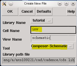
Go to the library manager. Click on File -> New -> cellview then select inv for cell name and composer-schematic. Click on OK.
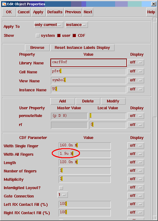
click on Add -> instance. Enter the Library as cmrf8sf. For cell you can put nfet for N_transistors and pfet for P-transistors you select.
Select the transistors and click property and change the width based on your layout, click OK.
In the schematic window select Add -> pin. Write down the pin names corresponding to your layout & make sure input/output type is selected properly.
You will find the vdd & gnd connections in Supply nets which is under the library analogLib.
Now to join all the components select Add Wire (narrrow only) and join all the components just like you would in a hand schematic.
Note
Make sure the bulk of pmos is connected to vdd and nmos to gnd.
When you are done, make sure to check and save your design by Clicking on Design -> Check and Save.
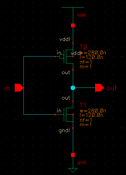
This is what an inverter schematic should look like.
Now the inv cell has both layout and schematic views. As a lowest level library cell, it needs two other important cell views.
- Symbol view: This view is necessary for schematic design entry. It is the symbol which represents the cell.
- Abstract view: This view is necessary for automatic layout (placement and routing) tools. It contains only cell boundary, I/O pin information, and metal obstructions. With this view the auto place and route tool will know where it can route without shorting existing metal contained in the cell.
3.3 Create Symbol View
If you want to use this cell as components in other design, you need to generate a symbol view for it. To do this
- From schematic menu, select Design 1 Create Cellview -> From Cellview ... This brings out a Cellview From Cellview window.
- Make sure Library Name is
tutorial, Cell Name isinv, From View Name isschematic, To View Name issymbol. Select Display Cellview and unselect Edit Options. Click OK.
A symbol view will be generated for this combinational logic according to its schematic view. Then the symbol view will be opened for you. After examine the symbol view, you may close it then save and close the schematic view.
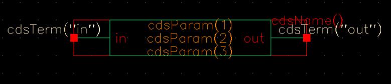
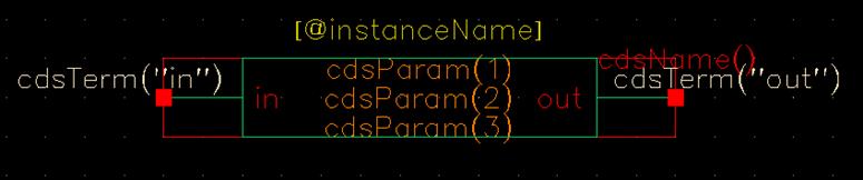
For convenience you may add a label of instance name on top of the symbol. Select Add -> Label, fill in [@instanceName] and place on top of the symbol.
3.4 Create Abstract View
You have to complete the layout view before you do this. If you change layout view later, you have to repeat the following steps.
There are three main steps in generating abstracts
generating the Pins view, the Extract view and finally the Abstract view.
- The Pins step maps text labels to metal layers, designating certain metal blocks as pins (We have laid out the pins, so we don't need to do anything in this step).
- The Extract step merges metal blocks under the same net into one single net. It also changes any metal.pin layer into metal.net.
- The Abstract step copies the pin (net) information from the Extract step, and generated blockages for the metal and via layers (or any other layer that you specify). These blockages will tell the place-and-route tool (namely Silicon Ensemble) which parts of the standard cell to avoid routing over with certain layers.
The resulting Abstract view contains only net and boundary (blockage) information.
Start Cadence with
icfb &
Open the inverter layout, select Tools -> Abstract Editor, This adds Abstract to the layout menu.
Now select Abstract -> Create Abstract, click OK in the pop-up window, the Abstract Generator will be opened.
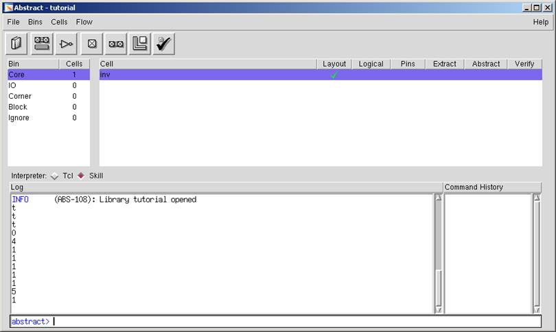
If your cell is in other bins instead of Core, you need to move it to Core bin. Select the cell you want to move, then click Cells -> Move, then choose Core, click OK.
-
The Pins Step
Select Flow -> Pin, fill in the window as the following picture:
We've already had the pins in the layout views, so we don't need to map text labels to pins
For DFF, put your clock pin name in the Clock pin names field
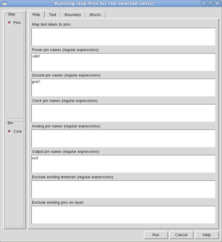
Choose the Boundary tab, do as followed:
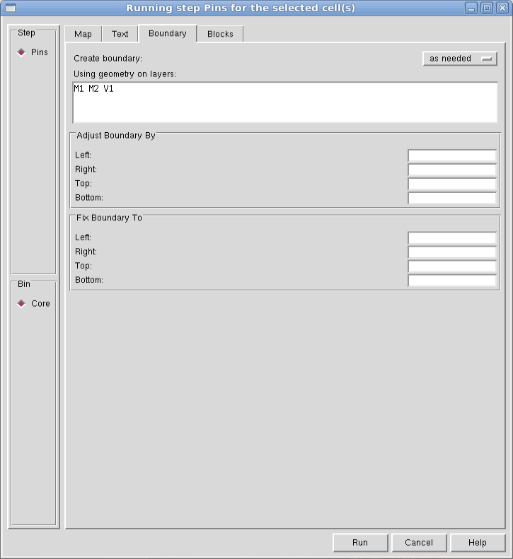
Then click Run. Abstract Generator will take a few moments to generate Pins views for the selected cell
After Abgen is done, you may see an exclamation mark (!) beside the selected cell, in the Pins column. An exclamation mark means that there was a warning (not an error) in the generation of that view.
There will be two warnings in the log window, reporting that the prBoundary does not enclose all cell view geometry and that no terminals created. Since we have created pins in the layout step, so just ignore the warnings.
-
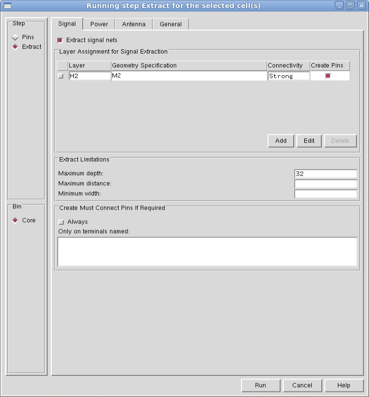
The Extract Step
Select Flow -> Extract, set the options in Signal tab as followed:
Power tab:
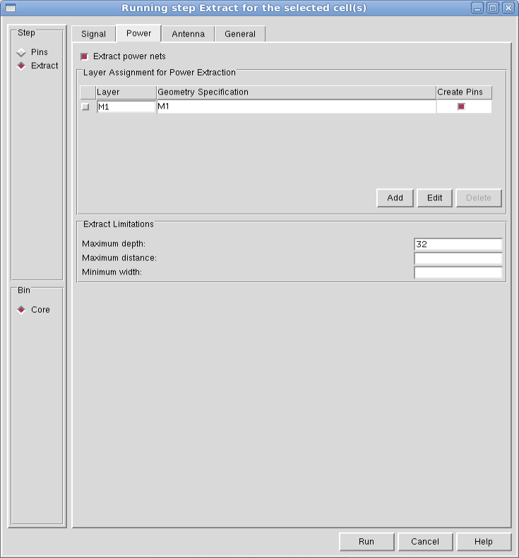
Don't do any change in the Antenna and General tabs.
Click on Run. You will see a green check mark in the Extract column in the main window.
-
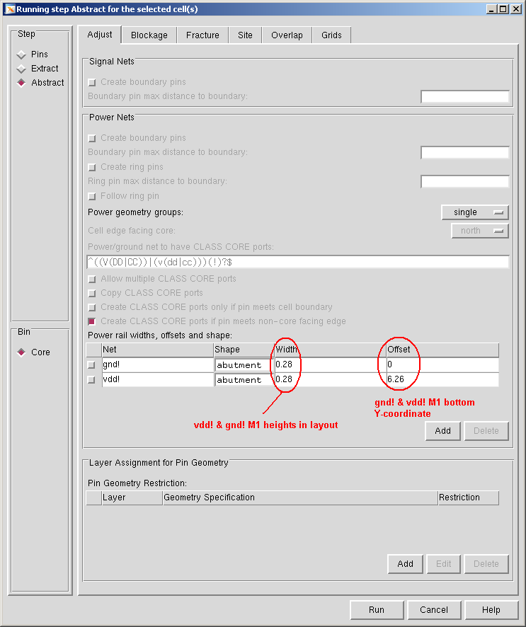
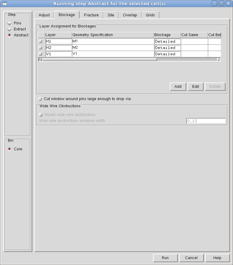
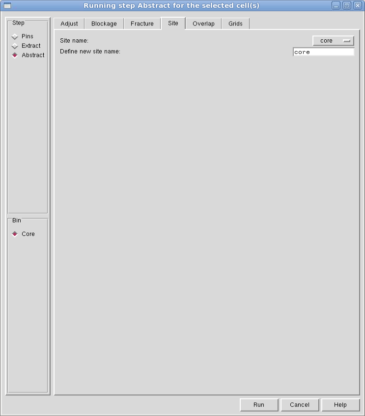
The Abstract Step
Select Flow -> Abstract, set the options in Adjust tab as followed:
Blockage tab:
Site tab:
Grid tab:
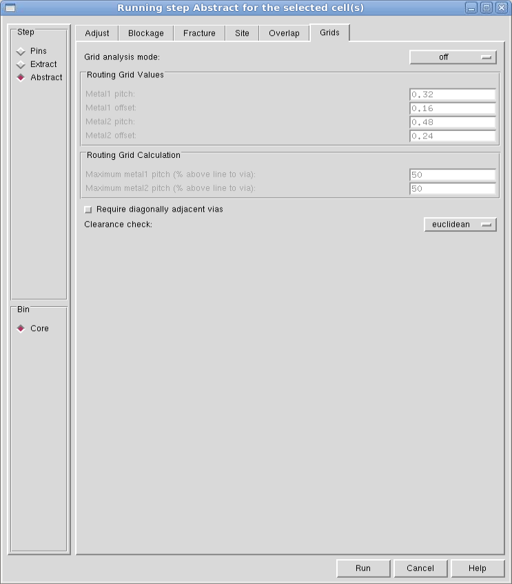
Click on Run.
The only warning is about the prBoundary y dimension. It's OK since we don't restrict the pitch in y dimension.
-
Hand Modify
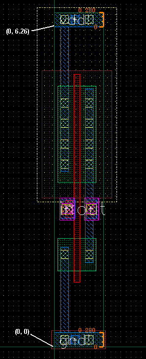
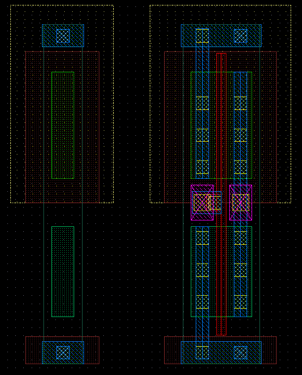
Now open the generated abstract view. It looks like below:
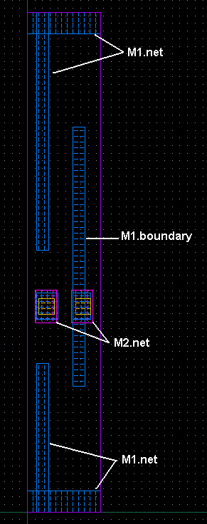
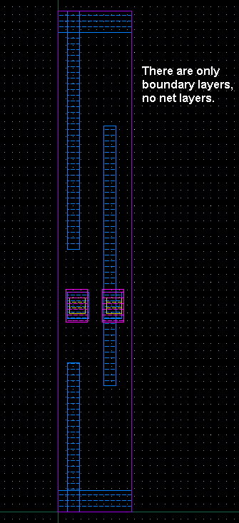
We need to change all net (nt for short) layers into boundary (by for short) layers. The final look of your abstract view should be as below. Make sure there are only boundary layers in your abstract view.
You can now save the abstract view.
4. Layout Verification and Extraction
4.1 Design Rule Check (DRC)
First of all, start cadence layout tools using icfb.
Open your inv layout view for editing.
Now we are going to check if there are any DRC errors in the layout.
From Virtuoso menu, select Assura -> run DRC..., this brings out a DRC window.
Put your Library, Cell and View names as picture below, or as your design.
For your Rules File, enter:
/proj/cad/library/mosis/IBM_PDK/cmrf8sf/relDM/Assura/DRC/drc.rul
Click Set Switches and choose BEOL_STACK_620, Cell, Ext_Latchup and GridCheck (hold the ctrl key while selecting).
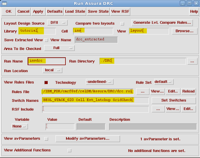
Click OK on DRC window. It takes a while to check all the DRC rules defined in the technology files.
When this window pop up at corner, wait until it complete.
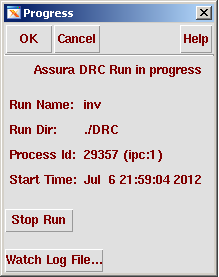
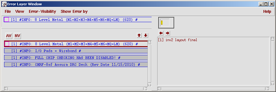
Click YES to see the result.
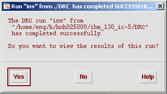
Ignore these warnings and infos, just fix all other errors.
After Fixing errors, Close your DRC runs by Assura -> Close Run
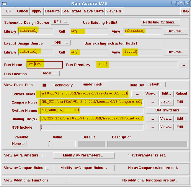
4.2 Layout vs. Schematic (LVS)
Layout vs. Schematic will compare your layout view with your schematic view.
Run DRC First, and make sure there is no error, and then Close your DRC runs by Assura -> Close Run.
To start LVS by Assura -> Run LVS.
You will see this window pop up. Put your layout and schematic information as this picture, or as your.
6 METAL PROCESS
For Extract Rules:
/home/cad/kits/IBM_CMRF8SF-LM013/IBM_PDK/cmrf8sf/V1.2.0.0LM/Assura/LVS/extract62.rul
For Compare Rules:
/home/cad/kits/IBM_CMRF8SF-LM013/IBM_PDK/cmrf8sf/V1.2.0.0LM/Assura/LVS/compare.cdl
For Switch Names:
Click Set Switches and then choose NO_SUBC_IN_GRLOGIC
For Binding FIles(s):
/home/cad/kits/IBM_CMRF8SF-LM013/IBM_PDK/cmrf8sf/relLM/Assura/LVS/bind.cdl
and then Click OK
4 METAL PROCESS
Note
Please use the 6 metal process for EE4325/6325 projects, the tech lef file for encounter is 6 metal, so always stick to 6 metal process.
For Extract Rules:
/proj/cad/library/mosis/IBM_PDK/cmrf8sf/relDM/Assura/LVS/extract41.rul
For Compare Rules:
/proj/cad/library/mosis/IBM_PDK/cmrf8sf/relDM/Assura/LVS/compare.cdl
For Switch Names:
Click Set Switches and then choose NO_SUBC_IN_GRLOGIC and resimulate_extracted
For Binding FIles(s):
/proj/cad/library/mosis/IBM_PDK/cmrf8sf/relDM/Assura/LVS/bind.cdl
and then Click OK
When this window pop up at corner, wait until it complete.
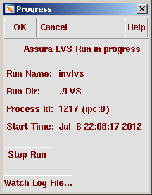
You will see similar pop-up window like this when the job is complete…
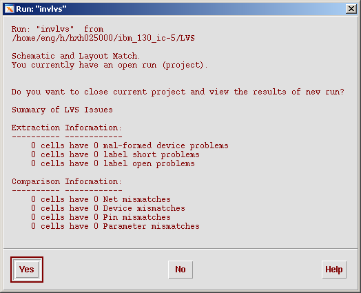
Make sure that the results say that the schematic and layout matches. If not, there is some problem in either the layout or schematic. Fix the problems in your layout and/or schematic.
Example:
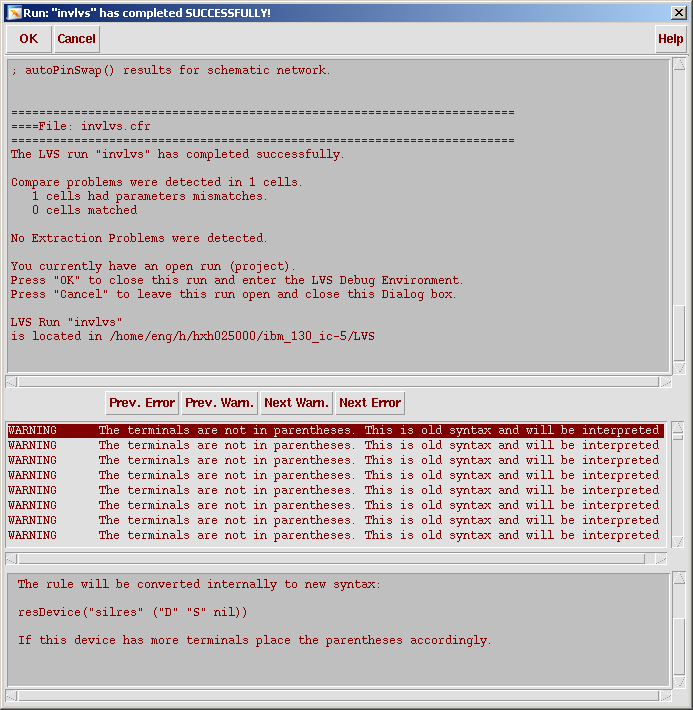
Click OK to enter the LVS Debug Environment.
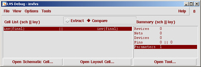
Go View -> LVS Error Report (Current Cell)
You will see the Error Report. Read it carefully and fix the errors in your schematic or layout. By clicking the node name or wire name, the corresponding part in the layout or schematic will be highlighted in the same color as the name.
If you change layout, you should do DRC again. Redo LVS until everything matches.
If you plan to go to extraction step, DON'T CLOSE THIS RUN!!! YOU HAVE TO HAVE LVS RUN TO DO EXTRACTION RUN!!! otherwise, close LVS run by: Assura -> Close Run
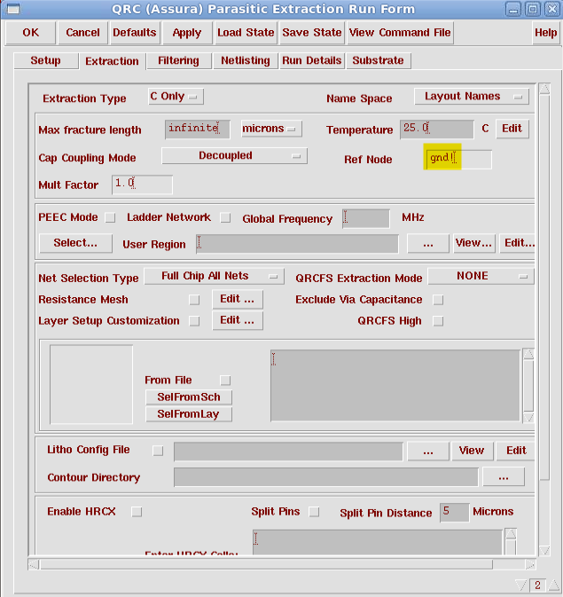
4.3 Practices Extraction (QRC)
Note
Make sure you run DRC and LVS FIRST, and NOT close LVS.
Go Assura -> Run QRC
You will see this Window, if it complains about missing technology directory put this for Setup Dir:
/proj/cad/library/mosis/IBM_PDK/cmrf8sf/relDM/Assura/QRC/41
Output should be Spice
Name is any name you want of your output netlist.
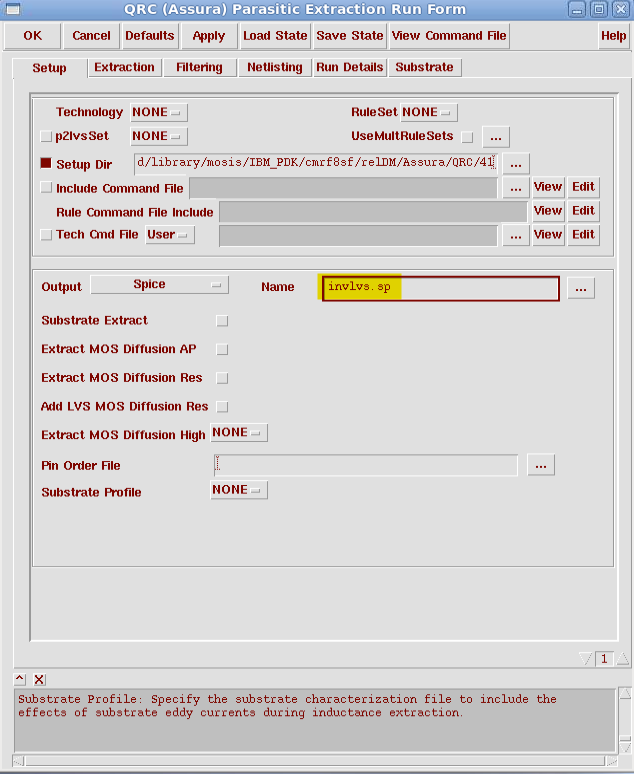
Go to Extraction tap, setup as below:
Go to Filtering tap, setup as below:
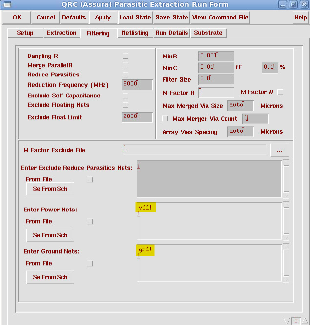
and then click OK.
QRC run completed successfully:
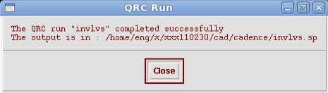
Once it is completed You will find the output file at your cadence working directory.
Your file will look similar to this: invlvs.sp
*
*
*
*                       LINUX           Sat Sep 30 03:39:33 2017
*
*
*
*  PROGRAM  advgen
*
*  Name           : advgen - QRC - (32-bit)
*  Version        : 9.1.3-p005
*  Build Date     : Tue Aug  3 12:36:00 PDT 2010
*
*  HSPICE LIBRARY
*
*
*
.GLOBAL gnd! vdd!
*
.SUBCKT inv in out
*
*
*  caps2d version: 10
*
*
*       TRANSISTOR CARDS
*
*
MT1 out in  gnd!    gnd!    nfet    L=0.12U W=0.4U
+ wt=4e-07 rf=0 nrs=0.619718 nrd=0.619718 ngcon=1 nf=1 mSwitch=0 m=1 blockParasiticsBetween="PC sub" PWORIENT=1 PLORIENT=1
MT0 out in  vdd!    vdd!    pfet    L=0.12U W=1.2U
+ wt=1.2e-06 rf=0 nrs=0.190476 nrd=0.190476 ngcon=1 nf=1 mSwitch=0 m=1 blockParasiticsBetween="PC sub" PWORIENT=1 PLORIENT=1
*
*
*       CAPACITOR CARDS
*
*
C1  vdd!    gnd!    1.2316E-16
C2  in  gnd!    4.72638E-16
C3  out gnd!    2.51092E-16
*
*
.ENDS inv
*
If your netlist comes with CAP/Diode CARDS following with some lines start with DavD, you need to comment out or delete them before HSPICE simulation.
Now, you can use HSPICE to simulation. You can work in the current cadence directory or spice directory after copying this output file there.
ADE Model
For people using Spectre(Cadence ADE), Spectre Model Library Location:
/home/cad/kits/IBM_CMRF8SF-LM013/IBM_PDK/cmrf8sf/V1.2.1.2LM/Spectre/models/allModels.scs
5. Final Design Preparation
5.1 Filler Design
Filler will be used by Encounter to fill the space between cells in each row. Without this, you may need to fix DRC errors manually at the end of encounter step.
Your filler should look like this:
Width (left boundary to right boundary) is your 1 pitch size. I used 0.48um for this example.
You draw dummy RX layer in PMOS and NMOS area for density rule check (not important for this project.. just incase).
Distance from boundary to RX layer in PMOS and NMOS has to be bigger than 0.1 um just like other cells in your library.
and don't forget to put VDD and GND pins (M1 pin layer).
Height of your cell, vdd rail, gnd rail, and all other layers height have to be equal with other cells in your library.
As shown this picture, all layers in filler have the same height and y-location with other cells. (This picture is just for comparison. DO NOT PUT YOUR INVERTER HERE!!)
Don't forget to make abstract view for filler!!
This filler will be used by encounter to fill the space between cells.
5.2 Preparing a synthesized Verilog netlist
If you haven't already developed a synthesized Verilog netlist, follow the instructions in Synthesis, with the following changes:
-
Change the library.lib Synopsys library file to match your cell library. If your cells differ from those in the library file, you may need to change cell names, pin names, and /or logical descriptions in the library file to match; this shouldn't be much of a problem if you pay attention to the Synopsys library file when laying out your cells in Cadence. Timing information is a more advanced subject, so you shouldn't change the given values, although you may want to experiment with changing the reported delays to match those of your cells if time allows.
-
Change the header.v Verilog header file to match your cell library. Although its format differs from that of the Synopsys library file, the syntactic format should be apparent.
-
Re-run Synopsys, attach the Verilog header, and verify your new synthesized netlist logically.
If you already have a synthesized netlist:
- Use a text editor with find & replace capability to replace all references to cell and pin names in your synthesized Verilog netlist to match those in your Cadence cell library. Pin names should only appear in the header section, while cell names appear throughout.
Or:
-
Rename each cell layout in Cadence to match the cell names listed in the Synopsys library file and Verilog netlist.
-
Rename each pin of each cell in Cadence to match those listed in the Synopsys library file and Verilog netlist.
-
Re-extract each cell.
Verify the functionality of your synthesized netlist. It is important to do this before continuing with the Encounter design flow, as functional errors at this level will propagate through the rest of the design steps.
Copy your final netlist into your Encounter working directory.
Example
If you have a rising-edge triggered dff that has an output qnot then you have to change your libary.lib file like this:
cell(dff) {
area : 7;
pin(d) {
    direction : input;
    capacitance : 1;
    timing() {
    timing_type : setup_rising;
    intrinsic_rise : 0.8;
    intrinsic_fall : 0.8;
    related_pin : "gclk";
    }
    timing() {
    timing_type : hold_rising;
    intrinsic_rise : 0.4;
    intrinsic_fall : 0.4;
    related_pin : "gclk";
    }
}
pin(gclk) {
    direction : input;
    capacitance : 1;
}
pin(rnot) {
    direction : input;
    capacitance : 2;
}
ff("IQ","IQN") {
    next_state : "d";
    clocked_on : "gclk";
    clear : "rnot'"
}
statetable ( "d rnot gclk", "qnot") {
        table :" - H ~R : - : N , \
                H/L H R : - : L/H ,\
                - L - : - : H " ;
}
pin(qnot) {
    direction : output;
    function : "IQN";
    internal_node : "qnot";
    timing() {
    timing_type : rising_edge;
    intrinsic_rise : 1.09;
    intrinsic_fall : 1.37;
    rise_resistance : 0.1458;
    fall_resistance : 0.0523;
    related_pin : "gclk";
    }
    timing() {
    timing_type : clear;
    timing_sense : positive_unate;
    intrinsic_fall : 1.29;
    fall_resistance : 0.0516;
    related_pin : "rnot";
    }
}
If you modifying your library.lib file, you need to redo Synthesis.
5.3 Preparing a Cadence Cell Library
Before you start, you need to:
-
Make sure to verify the functionality of each cell with the Cadence DRC and SPICE simulation,
-
Make sure your cells match the logical descriptions in the Verilog header and Synopsys library file with regard to input pins (i.e.: if the aoi12 is (a+(b c))' in the Synopsys library file and is ((a b)+c)' in Cadence layout, the final routed circuit will have a logic error).
-
Make sure you have abstract views for each cell as well, and that your Cadence physical library contains only cells you wish to use for your cell library. It is important to make sure that your cells are correct.
Now, from your Cadence directory, copy the LEF modifier script and header by typing (there is a space after cp and after the name then a period):
cp /home/cad/startup/EE6325/aux/native_abs.pl .

cp /home/cad/startup/EE6325/aux/strmoutMap .

cp /home/eng/x/xxx110230/public_html/scripts/ibm130/native_header.lef .
5.3 Library Exchange Format(LEF)
An ASCII data format, used to describe a standard cell library.
LEF Generation
To get .lef file, you have use another version of ibm130 technology. To do that, follow these steps:
At the cadence folder
Edit your cds.lib, it should be like this:
DEFINE cdsDefTechLib $CDS_INST_DIR/tools/dfII/etc/cdsDefTechLib
DEFINE analogLib $CDS/tools/dfII/etc/cdslib/artist/analogLib
DEFINE basic $CDS/tools/dfII/etc/cdslib/basic
DEFINE cmrf8sf /proj/cad/library/mosis/IBM_PDK/cmrf8sf/V1.8.0.4DM/cdslib51/cmrf8sf
DEFINE esd8rf /proj/cad/library/mosis/IBM_PDK/cmrf8sf/V1.8.0.4DM/cdslib51/esd8rf
DEFINE avTech /proj/cad/cadence/assura-5141-3.20.001.lnx86/tools/assura/etc/avtech/avTech
DEFINE "your_library and path"
After you are done with creating .lef file and .asc file, you may delete or comment out the line of avTech.
Exporting LEF File
After sourcing the profile, start Cadence from your Cadence directory by typing:
icfb &
Since Encounter runs as a stand-alone design tool, you will need to export your cell library in the LEF file format for Encounter to read. The LEF format contains pin connectivity and cell size information for your library.
Un the CIW window select File -> Export -> LEF. In the window that appears, enter the desired LEF file name (with extension ".lef"), select Overwrite Existing LEF File, make sure the cmrf8sf technology library is selected, and select Logical & Physical, Silicon Ensemble, and Overwrite Cell List File.
Now click the Pattern Match button at the bottom of the window, enter the desired library name and click OK to close the window.
Click OK to begin generating the LEF file.
You may need to modify the lefout.list file based on your needs. It should be in the format of:
Library_name cell_name abstract
For example:
vlsi inv abstract
vlsi nand2 abstract
vlsi nor2 abstract
Check your output .lef file to see if it contains MACRO information for each cells in your library. E.g.:
MACRO nand2
    CLASS CORE ;
    FOREIGN nand2 0.00 0.00  ;
    ORIGIN 0.00 0.00 ;
    SIZE 1.44 BY 6.54 ;
    PIN a
        DIRECTION INPUT ;
        PORT
        LAYER M2 ;
        RECT  0.14 2.61 0.34 2.81 ;
        END
    END a
    PIN out
        DIRECTION OUTPUT ;
        PORT
        LAYER M2 ;
        RECT  1.10 2.61 1.30 2.81 ;
        END
    END out
    PIN b
        DIRECTION INPUT ;
        PORT
        LAYER M2 ;
        RECT  0.62 2.61 0.82 2.81 ;
        END
    END b
Exporting ASCII Dump file
Now select File -> Export -> Stream in the CIW window.
Enter your library name and library cell name in the resulting window. Make sure the view name is layout, and select ASCII Dump and enter an output filename (with extension ".asc"). Make sure Units is set to micron and click OK to generate an ASCII physical description file.
Now click the User-Defined Data button on the Stream-out form, which should open the following window:
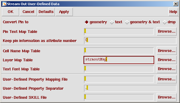
And enter strmoutMap for Layer Map Table as shown above. Hit OK to run the stream export.
Click OK to close the main stream-out window and generate an ASCII physical description file.
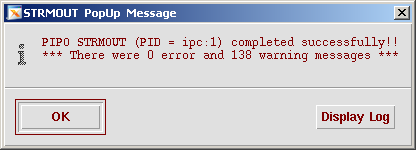
If you get warnings, ignore them for now. If the export fails, check your settings and try again.
Quit Cadence. Both the LEF and ASCII files are located in your Cadence working directory (see above).
Converting LEF file
Now, run the native_abs.pl script. This script converts your LEF file to a format that Encounter can read, and uses physical information from the ASCII file to warn the auto-routing tools about extraneous metal objects. Invoke the script by typing:
perl native_abs.pl
Enter native_header.lef for the technology header filename, and your LEF and ASCII files for the following file prompts, followed by an output filename (with extension ".lef"). Select the defaults for all the following prompts (assuming your power/ground pins are named vdd! and gnd!), and select n for both symmetry options. It will ask you for pitch spacing. This is where you will enter the uniform distance between your pins. (i.e. if you separated your pins with a multiple of .8 then enter .8 for your pitch). The script should produce a modified LEF file for import into Silicon Ensemble. Copy this file into your Encounter working directory. Here is some sample output, be sure to change the file names to what you used to output these files. Make sure you put in the correct pin spacing as well.
This script file modifies an abgen .lef file for use with Encounter:
Four files are necessary for proper .lef conversion:
1. Technology file - provided - provides header information
2. LEF file - you generated from Abstract views and Cadence - provides cell macro data
3. ASCII dump file - you generated from Cadence - provides obstruction data
4. Output file - existing or created now
Please enter technology header file name: native_header.lef
Please enter your abgen file name: test_lib.lef
Please enter your ascii dump file name: test_dump.asc
Please enter output file name: test_out.lef
Test_out.lef created!
Please enter global power pin name or
Please enter global ground pin name or
Please enter global clock pin names separated by spaces or
Please enter global signal pin names separated by spaces or
Please enter horizontal rail pin names separated by spaces or
X symmetry for all cells[y/n]? n
Y symmetry for all cells[y/n]? n
Please enter pin pitch: 0.48
Writing header...
Done!
Writing site data...
WARNING: cell dff boundary height is off-grid!
WARNING: cell inv boundary height is off-grid!
WARNING: cell filler boundary height is off-grid!
WARNING: cell nand2 boundary height is off-grid!
WARNING: cell nor2 boundary height is off-grid!
WARNING: cell xor2 boundary height is off-grid!
Writing macro dff...
No obstruction information found
Writing macro inv...
No obstruction information found
Writing macro filler...
No obstruction information found
Writing macro nand2...
No obstruction information found
Writing macro nor2...
No obstruction information found
Writing macro xor2...
No obstruction information found
If you get height warning errors ignore them, if you get errors about off-boundary pins double check your pin spacing in all your settings and make sure that they are uniform. Width errors may mean you need to check your prBoundary. Check your pin spacing/cell boundary spacing so cells can be placed next to each other with no errors. You must make sure the script outputs information for each of the cells in your library.
Now you can proceed to the encounter tutorial.
6. Design Verification
6.1 Design Entry by Verilog Netlist
You don't have the schematic view of your complete design in your own library, please import the Verilog Netlist first.
Make sure all the cells in your library have their symbols which were generated from the schematic view.
To generate symbol view, open your schematic view and click: Design ->Create Cellview-> from Cellview and then just click OK. Now you will see symbol view of your cell.
After you have done this for all your cells.
You need to import the Verilog file into Cadence, To do that start Cadence i.e "icfb". Then
-
From CIW, select File -> Import -> Verilog ... This brings out a Verilog In form.
-
Fill in your project library name as Target Library Names, "YOUR VERILOG FILE WITH LOCATION (can be../se/YOUR_SYSTEM_map.v)" as Verilog Files To Import.
-
Click OK.
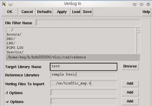
It takes a while to complete the import process. You can monitor the progress in CIW.
This process generates schematic and symbol views for combinational logic according to the verilog netlist.
After that, you should open your schematic view of your design in Cadence, replace every netname "GND!" to "gnd!", and "VDD!" to "vdd!".
Use the Edit -> Search -> Replace option.
Do not forget to click check and save button, or your LVS check may fail!!
6.2 Import .def File
Note
Before you import your .def file into cadence, make sure your are pointing to the correct cmrf8sf in your cds.lib
It should be defined as:
DEFINE cmrf8sf /home/cad/kits/IBM_CMRF8SF-LM013/IBM_PDK/cmrf8sf/V1.1.0.6LM/cdslib/cmrf8sf
Make sure you sourced the cad profile and start cadence.
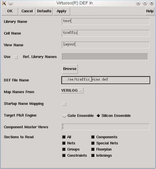
In the CIW window, select File->Import->DEF.
Enter the library name of your cell library, the cell name of your design (the name of your top level module is a good idea), and Layout for View Name.
Enter the location and name of the .def file, make sure that Target P&R Engine is set to Silicon Ensemble and Sections to Read is set to All. Click OK.
6.3 Change the view
Open the newly imported Layout view. The cells will be displayed in abstract views. You need to replace abstract views with layout views after .def import.
Click Tools->layout, then click Design->Remaster Instances, set the ViewName as follows, and then click OK.
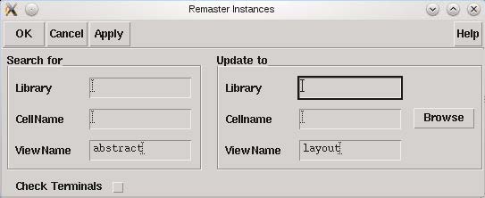
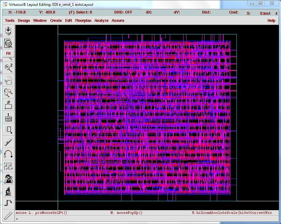
Now you will be able to see the layout in layout views.
6.4 DRC Check
Run DRC check as before, but you will probably get several errors like below:
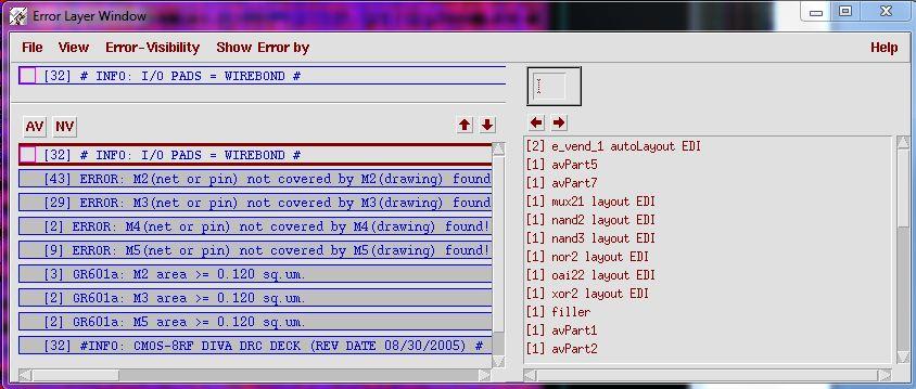
These DRC errors are related to the pins placed by Encounter during the placement and routing process. Encounter puts the pin with the name of the signal at the end of the metal wire that connects to that pin.
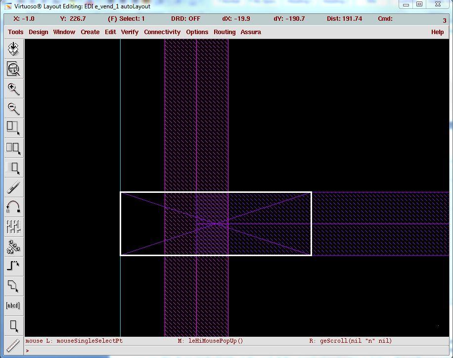
You can see this if you look closely at the end of the signal wires in picture below, the ends are not filled in like they would be in metal layer.
To fix these run the pin_cover.tcl script, you won't have these errors if you already did this.
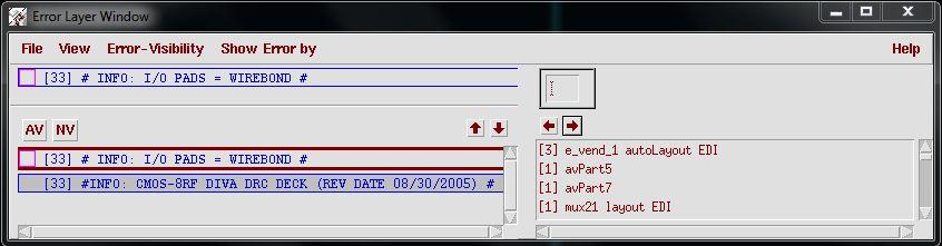
Fix any other errors, you should get no DRC errors. You can ignore these two information.
6.5 LVS Check
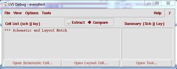
Run LVS check as before, make sure pick the 6 Metal rules.
Make sure that your layout and schematic match. If they don't possibly debug all the errors yourself!!
If LVS failed because of this error
*ERROR* Device 'cds_thru(RES)' on Schematic is unbound to any Layout device.
Use the following Compare Rules
/home/eng/x/xxx110230/public_html/scripts/ibm130/compare.cdl
Comment
Create Rectangle has bind key r, and it is listed in graphic tool bar too.