65nm Process - GF65 PDK
0. Environment setup
Create your working directory;
mkdir -p ~/cad/gf65 && cd ~/cad/gf65
Setup for GF65 PDK, only need run once;
/proj/cad/startup/setup-gf65_lpe.ic-6
1. Start Cadence
Go to Cadence working directory
cd ~/cad/gf65
Each time you open a terminal to start Cadence for GF 65nm PDK, you need source this profile.
. /proj/cad/startup/profile.ee7325
If you went thru the setup section, You should have library, display and rule files for cadence. If you haven't setup, please redo section 0. environment setup.
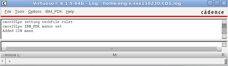
Start Cadence by:
virtuoso &
The first window that appears is called the CIW (Command Interpreter Window).
Now you can open the Library Manager through Tool -> Library Manager you can manage your design process and use various Cadence features. This window shows reference libraries including analogLib, cdsDefTechLib, basic, esd10lpe, and cmos10lpe. Make sure that all of these libraries show in the Library Manager window. You will use analogLib for building schematic views. cmos10lpe is the technology library for the GF65nm Process.
To quit Cadence, select File -> Exit. A message window appears to confirm your command. Select OK to exit.
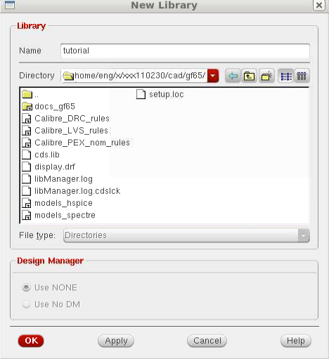
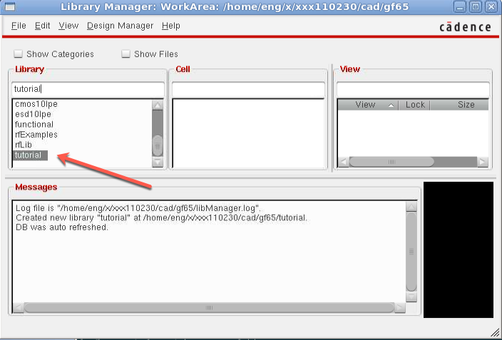
2. Create a Design Library
Design libraries are the places where you store your designs. The first step of IC design in Cadence is to create a design library so you can develop your design. Now we are going to create a design library called tutorial then put the design of the inverter in it.
From pull-down menu in Library Manager, select File -> New -> Library.... This will bring out a Create Library box.
Enter tutorial as the name, and click OK
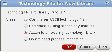
Then a new box will pop up. If not, you may find it at bottom taskbar.
Choose Attach to an existing tech library
Then choose cmos10lpe and click OK.
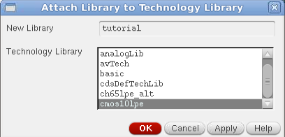
The technology file is then compiled and the library tutorial is created.
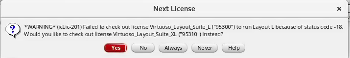
Ignore warnings about License, click Yes and move on, or Always.
3. Create different cell views
Once you have created a design library, you can start to put your design into it. We are going to design a inverter (INV) as example
3.1 Create Layout view
To create a cell named inv in library tutorial
1.First click on tutorial in Library catalog
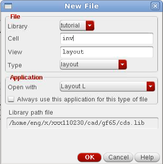
2.Select File -> New ->Cellview ..., if it is gray out and you can't click it, DO STEP 1
3.New File box pops up.
Select tutorial as Library Name;
Enter inv as Cell Name;
Enter layout as View Name;
Select layout as Type then click OK.
If you are asked by some license related questions, choose Yes or Always.
4.Cell inv with layout view in library tutorial will be created and opened up for you to edit.
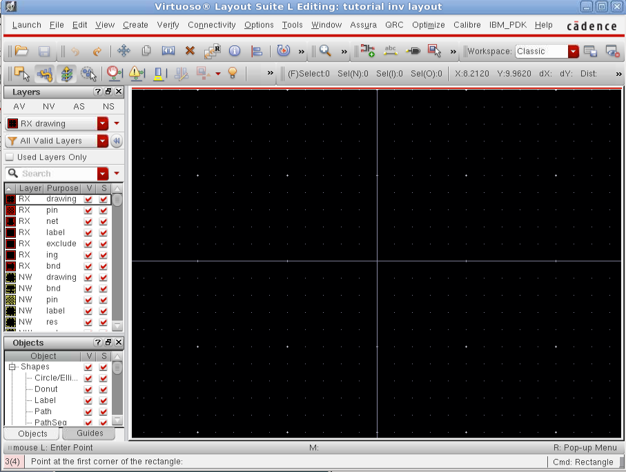
The most common shape in a layout is rectangle. From LSW select a layer by clicking left mouse button on it. You will see the selected layer surrounded by wider border (the selected layer is highlighted), like M1 drawing is metal1 layer with drawing purpose
From Virtuoso Layout Editing window pull down menu, select Create -> shape -> Rectangle
Tip
Create Rectangle has shortcut R, and it is also listed in menu.
In the layout design window (Virtuoso Layout Editing) click left mouse button for the first corner of the rectangle, then click left mouse button again for the second corner. A rectangle is drawn.
- If this is not the desired rectangle, select Edit -> Undo from menu to undo the action.
- If you want to draw another rectangle using current drawing layer, simply click left mouse button for the two corners of the rectangle.
- If you want to draw rectangles of another layer, click left mouse button to select your layer in LSW to change the drawing layer then click left mouse button for the two corners in Virtuoso Layout Editing window.
- If you have finished drawing rectangles, press <
Esc> on the key board to exit from "Create Rectangle" command.
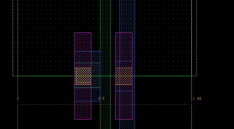
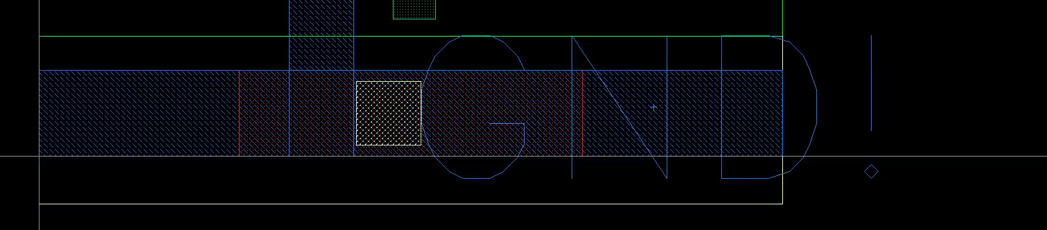
5.Click on NW drawing in the layers window and create a rectangle which looks like the picture shown below. Do not worry about sizing for now this is just a tutorial, however, you need to worry about the sizes for the actual layout.

6.Click on RX drawing layer and create four rectangles as shown. Two of the rectangles will reside in the NW, and the other two will be outside the NW.
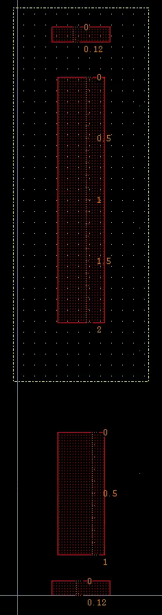
7.Click on JZ drawing layer and create two rectangles as shown. One rectangle will surround the second RX, and the other will surround the fourth RX.
8.Click on JX drawing layer and create two rectangles as shown. They will surround the other two RX rectangles.
9.Click on PC drawing layer and create a rectangle crosses the middle two RX rectangles as shown.
10.Click on CA drawing layer and create rectangles as shown.
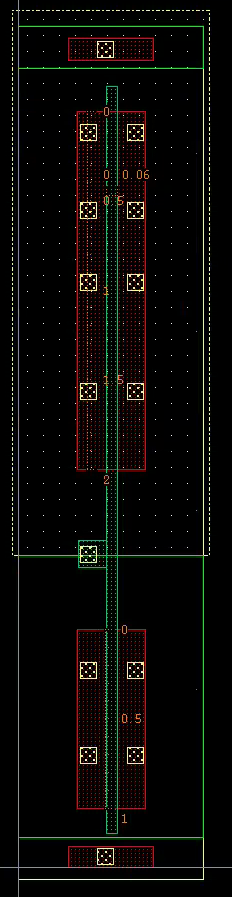
11.Click on M1 drawing layer and create rectangles as shown.
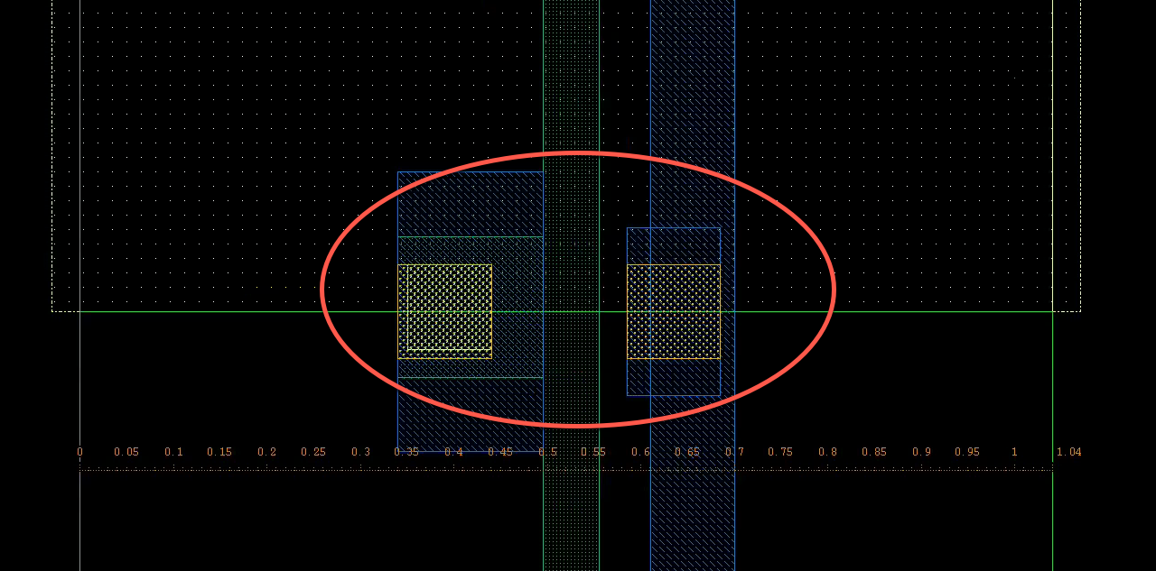
12.Click on V1 drawing layer and create rectangles as shown, there are TWO V1 rectangles in red circles, and you don't need to drawing those circles.
13.Click on M2 drawing layer and create rectangles as shown.
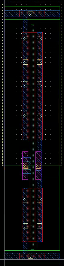
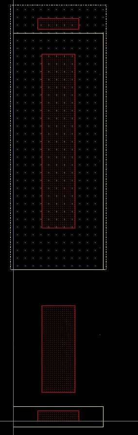
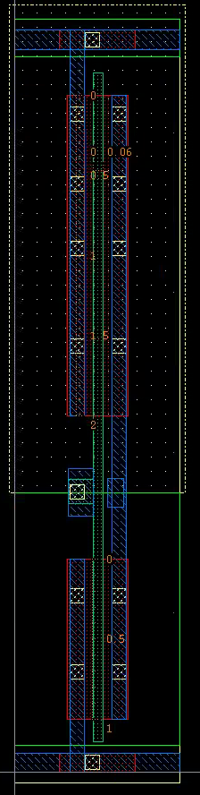
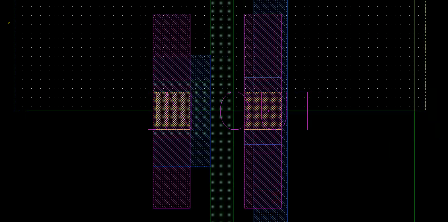
14.Putting Pins
Pins define where the wires outside the cell can be connected to the cell. In our example, we need pins for IN, OUT, VDD! and GND!. And VDD! an GND are connectted with M1, which goes horizontally between cells, IN and OUT are connectted with M2, which goes veritically between cells.
To create all of these pins:
14.1 For Vdd and Gnd
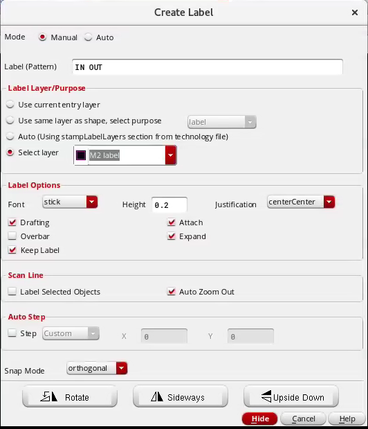
- Select Create -> Label... . This brings out the "Create Lable" form
- Fill in
VDD!orGND!in Label(pattern), Select Layeris M1 label,Label Heightis 0.2.
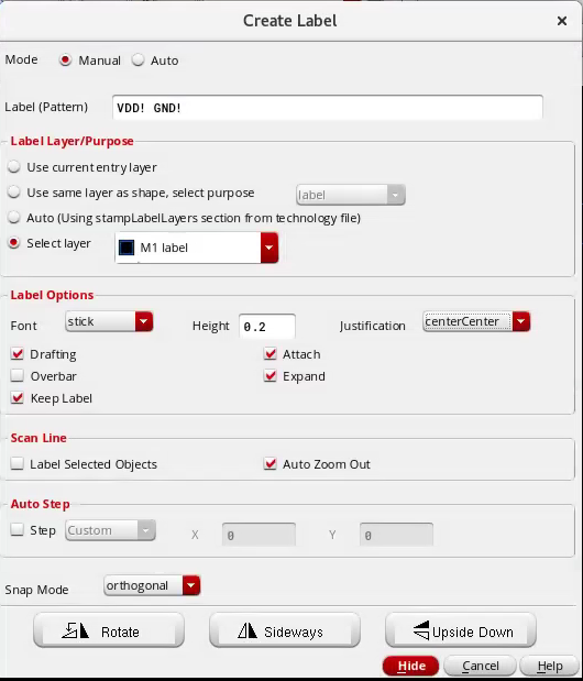
Put labels in the pin area as shown,and you don't need to drawing those circles.
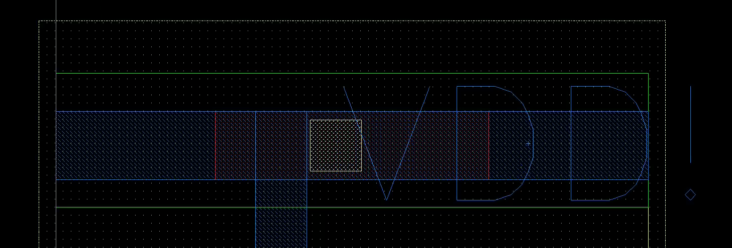
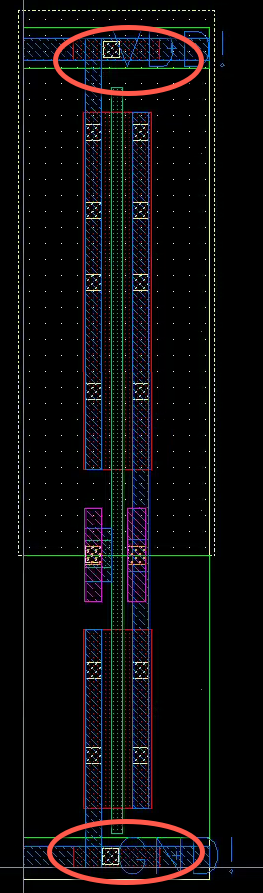
14.2 For Input and Output
- Select Create -> Label... . This brings out the "Create Lable" form
- Fill in IO names in Label(pattern), and there is not difference between input and output.
Select Layeris M2 label,Label Heightis 0.2.
Put labels in the pin area as shown.
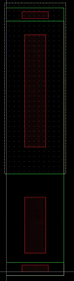
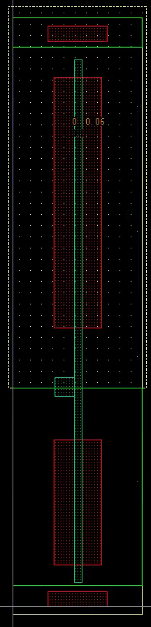
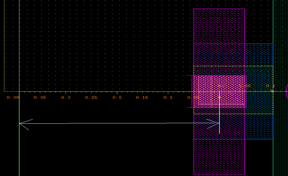
The pin pitch should be (0.26*n), meaning it can be 0.26, 0.52, 0.78...
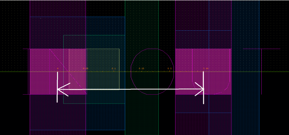
The offset should be (0.13 + 0.26*n), meaning it can be 0.13, 0.39, 0.65...
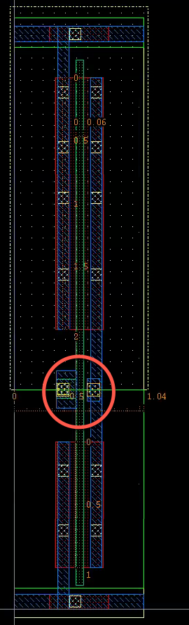
15.For P&R later, add prBoundary(purpose boundary) layer and Cell height should be odd multiple of pin pitch size.
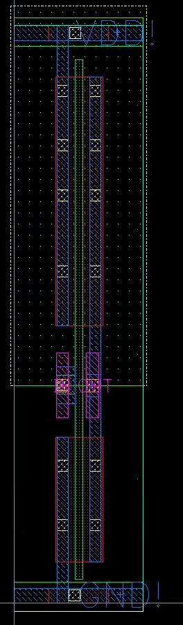
Your final inverter layout should be similar to this, now you can start to run DRC
Disable Gravity
It is highly recommended to disable Gravity, select Options -> Editor
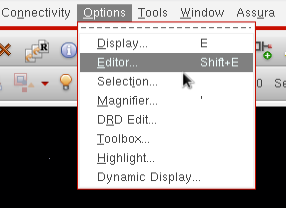
then uncheck Gravity On and choose Types as None
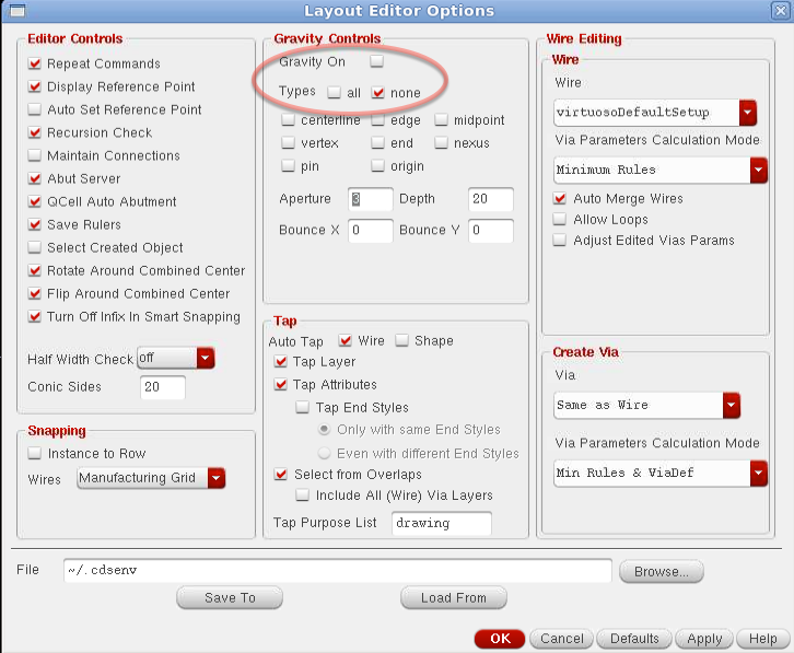
Shortcut g is toggle of this option. If you disable it at beginning, and press g afterward, it will turn on again.
Layout Design Rules
To check the layout design rules, put this commands in your terminal
acroread ~/cad/gf65/layout_rules_rev9 &
And read Chapter 3 Physical Design Rules starts at page 63.
Layout Shortcuts
| Shortcut | Function |
|---|---|
u |
undo |
ctrl z |
zoom in , or zoom by drawing a box around the zoom area with right mouse button. |
shift z |
zoom out, shift + draw box with right mouse button ----> zooms out really fast |
r |
draw rectangle |
s |
stretch the edge of an item (must be in Partial Select mode) |
m |
move. Press F3 after to see all the move options, like rotate & flip |
c |
copy. Press F3 to see the move options, like copying multiple times |
p |
Used for drawing path lines, and is much better than rectangles. Press F3 to see path options, like path width, or try using partial select to modify the length of the path after you've drawn it. |
i |
insert - instance (=adds a cell) |
k |
ruler. Press F3 for more options, like auto-snap opitions |
shift k |
delete all rulers |
f |
fit entire layout to the screen |
shift f |
display all levels of hierarchy (You can also do this by going to the Virtuoso Options menu, choosing Display and setting Display Levels from 0 to 32) |
ctrl f |
switch back previous step, or set the Display Levels back to 0 from the Options menu. |
| g | toggle gravity on/off, normally you want it OFF |
shift c |
chop =cuts pieces out of a selected item. Press F3 for more options |
shift m |
merges selected items (must be overlapping) |
ctrl r |
redraw |
ctrl p |
insert pin (more on below) |
x |
edit in place |
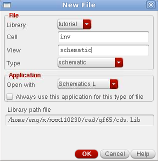
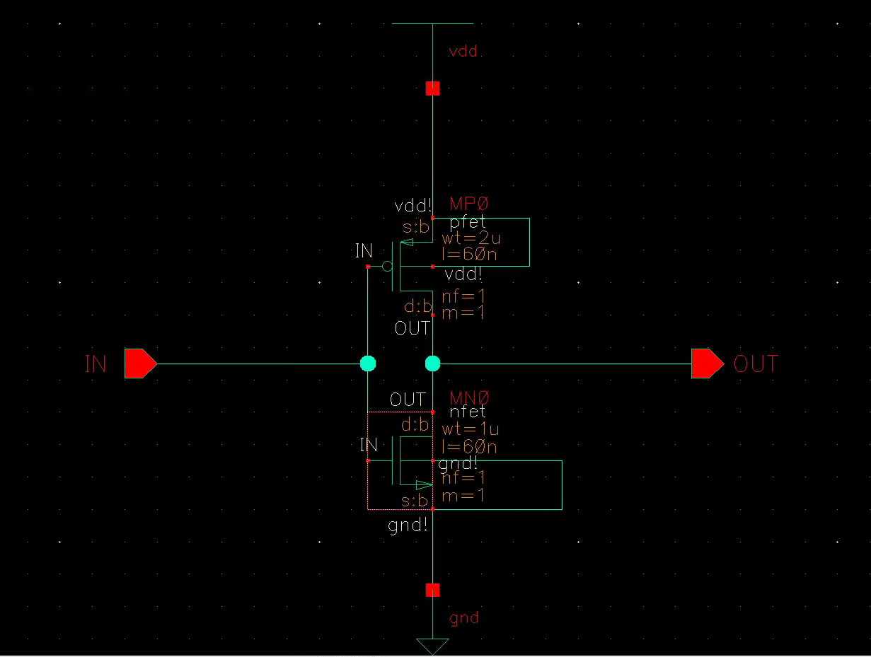
3.2 Create Schematic view
Go to the library manager. Click on File -> New -> Cellview ..., then type inv for Cell and schematic for View. Click OK.
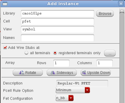
click on Create -> instance. Enter the Library as cmos10lpe. For cell you select pfet for P-transistors and nfet for N-transistors.
Now to join all the components select Create -> Wire (narrrow only) and connect all the components just like you would in a hand schematic.
Tip
Make sure the bulk of pmos is connected to VDD! & nmos to GND!.
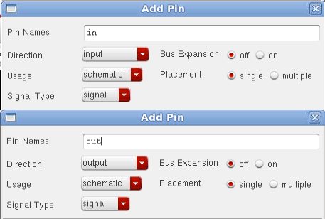
In the schematic window select Create -> pin. Enter pin names corresponding to your layout & make sure input/output is selected properly.
You will find the VDD! & GND! in library analogLib. Then select Creat -> Wire (narrrow) and join all the components just like you would in a hand schematic.
Your schematics should be similar to this, check and save your design by Clicking on File -> Check and Save.
4. Layout verification and extraction
After we layout a cell. we need to perform a design rule check (DRC). Passing the DRC means your layout is meeting the fabrication standard. However the functionality of the cell many NOT be correct. We need to run layout vs. schematic check (LVS) to make sure the layout is equal to the schematic. After the LVS is done, we need to extract all the parasitic capacitance and resistance of the layout by running PEX. With the extracted information, we can now simulate the layout of the cell.
4.1 Design Rule Check (DRC)
First of all, start cadence layout tools using virtuoso and open your inv layout view for editing.
Now we are going to check if there are any DRC errors in the layout. The layout DRC rules are summarized by the design rules shown above. If you know what could be wrong in the layout, you can try to fix it/them and verify your modified layout by DRC. If not, let's go on to verification.
From Virtuoso menu, select Calibre -> run DRC
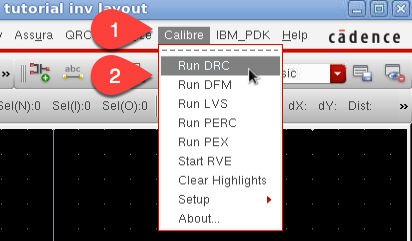
When it ask for runset file just click cancel. We will set the file later.
There are several options you need to set. For options not mentioned below, leave them as default at normal case, we may change them in future if neccessary.
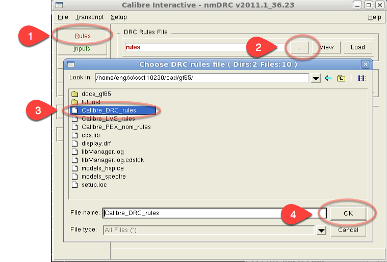
Click Rules tab first, DRC Rules File is located in the gf65 folder in your home directory, named Calibre_DRC_rules
You can set the DRC Run Directory to anywhere. I recommend to create a new subfolder and then all DRC files will be stored there, e.g. yourcellname_DRC.
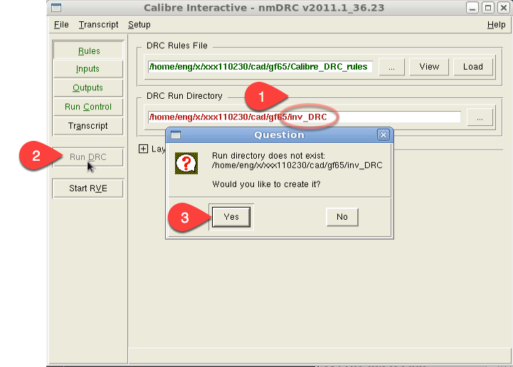
Now click the Run DRC and it will start to run DRC. It may ask you if create unexist directory and click Yes, or click Ok when it ask if overwrite files.
Calibre RVE should pop up after DRC running finished, and from there, you can see if your layout violate any design rules. Calibre calls DRC error as Result, if you see some number of Results, it means your layout has DRC errors, highlight and come back to Layout editor to fix them, until no error.
If you get some density-related DRC error, contact with TA to confirm if you could ignore it, but you still need to fix all dimension-related DRC errors.

4.2 Layout vs. Schematic check (LVS)
Layout vs. Schematic check will compare your layout view with your schematic view.
Run DRC first, and make sure there is NO error and then Close your DRC runs.
From Virtuoso menu, select Calibre -> run LVS
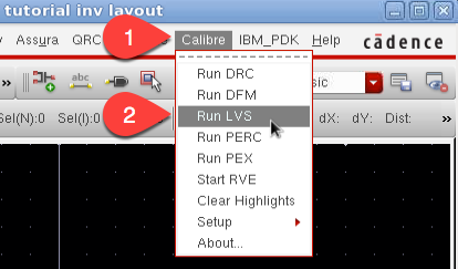
When it ask for runset file just click cancel. We will set the file later.
There are several options you need to set. For options not mentioned below, leave them as default at normal case, we may change them in future if neccessary.
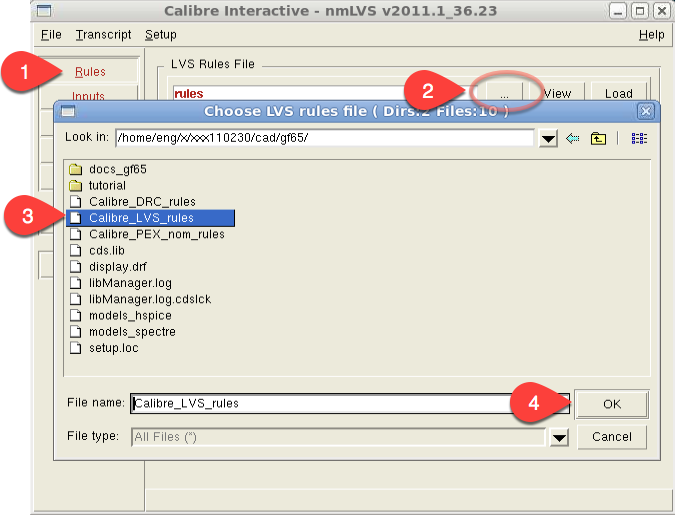
Click Rules tab first, LVS Rules File is located in the gf65 folder in your home directory, named Calibre_LVS_rules
You can set the LVS Run Directory to anywhere. I recommend to create a new subfolder and then all LVS files will be stored there, e.g. yourcellname_LVS.
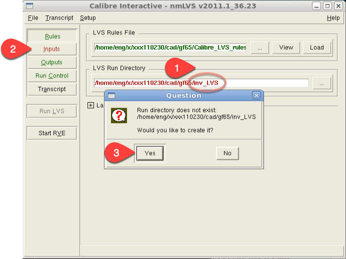
Click on Inputs tab, it may ask you if create unexist directory and click Yes. And click on the middle Layout tab, make sure that
-
Export from layout viewer is checked.
-
Top cellis the cell name which LVS is running
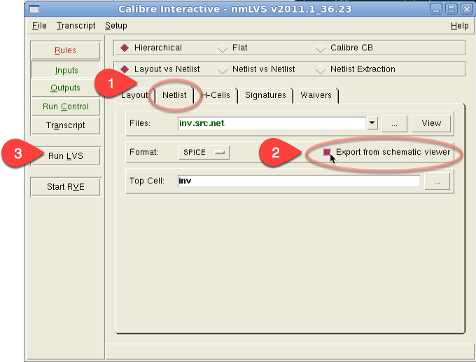
Now click the Run LVS and it will start to run LVS, click Ok when it ask if overwrite files.
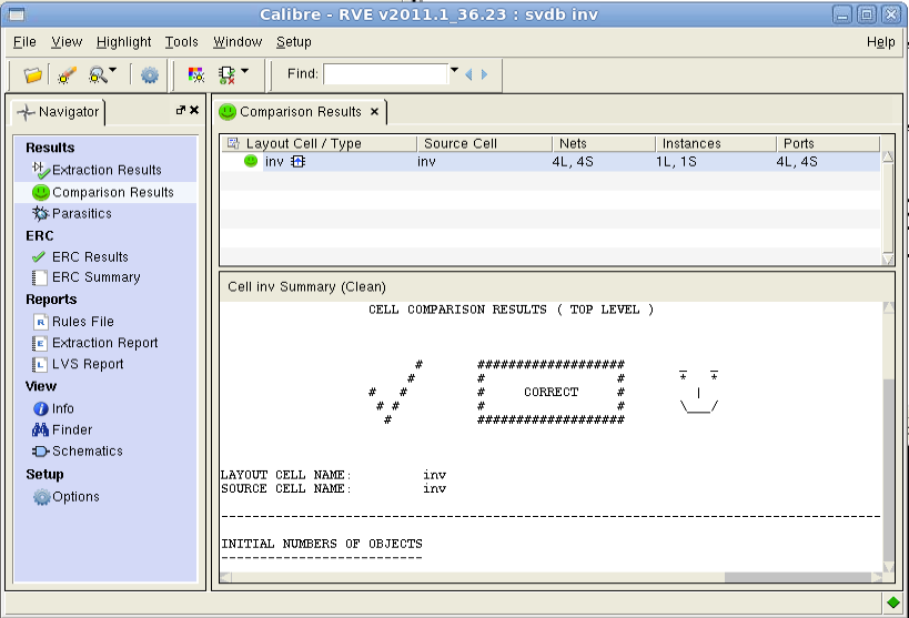
Make sure that the results say that the netlist matches the schematic. If not, there is some problem in either the layout or schematic.
Fix the problems in your layout and/or schematic. If you fixed layout, make sure you extract again. Redo LVS until everything matches.
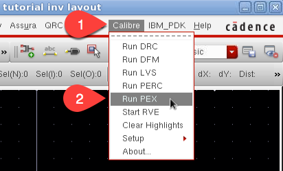
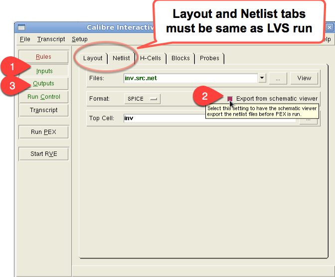
4.3 Parasitic Extraction (PEX)
Now we're going to extract the parasitic wire capacitances and resistances from the layout.
To perform Parasitic Extraction(PEX), choose Calibre -> Run PEX
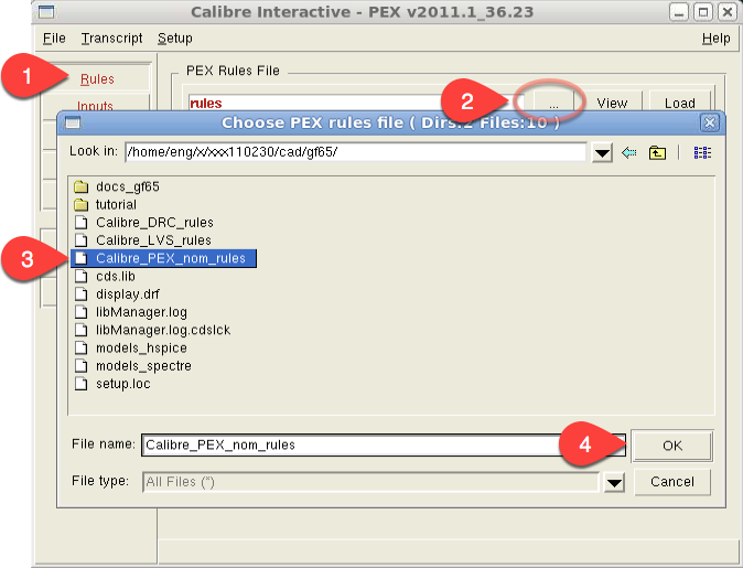
There are several options you need to set. For options not mentioned below, leave them as default at normal case, we may change them in future if neccessary.
Click Rules tab first, PEX Rules File is located in the gf65 folder in your home directory, named Calibre_PEX_nom_rules
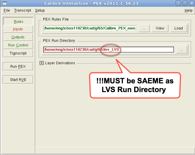
Make sure that set PEX Run Directory exactly as LVS Run Directory of your cell want to extract.
In Inputs tab, make sure Layout and Netlist tabs setup same as LVS run
- Under the
Netlisttab, check the option "Export from schematic viewer"
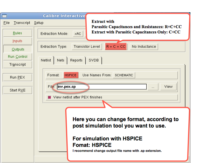
In Outputs tab, for simulation with HSPICE, setup as below, or you can setup based on your need.
-
Format:
HSPICE -
I recommand change output File name extension to
.sp
Now, you can use HSPICE to make simulation with your extracted .sp file, which is inside LVS working folder, inv_LVS as example, in the current gf65 directory.
Example extracted spice netlist file
* File: inv.pex.sp
* Created: Tue Jun 20 17:07:09 2017
* Program "Calibre xRC"
* Version "v2011.1_36.23"
*
.include "inv.pex.sp.pex"
.subckt inv  GND OUT VDD IN
*
* IN    IN
* VDD   VDD
* OUT   OUT
* GND   GND
XD0_noxref N_GND_D0_noxref_pos N_VDD_D0_noxref_neg DIODENWX  AREA=1.41141e-12
+ PERIM=4.754e-06
XMMP1 N_OUT_MMP1_d N_IN_MMP1_g N_GND_MMP1_s N_GND_D0_noxref_pos NFET L=6e-08
+ W=1.5e-07 AD=2.76e-14 AS=2.625e-14 PD=6.68e-07 PS=6.5e-07 NRD=0.666667
+ NRS=0.666667 M=1 NF=1 CNR_SWITCH=0 PCCRIT=0 PAR=1 PTWELL=0 SA=1.75e-07
+ SB=1.84e-07 SD=0 PANW1=0 PANW2=0 PANW3=0 PANW4=0 PANW5=0 PANW6=4.62e-15
+ PANW7=4.38e-15 PANW8=0 PANW9=0 PANW10=0
XMMP0 N_OUT_MMP0_d N_IN_MMP0_g N_VDD_MMP0_s N_VDD_D0_noxref_neg PFET L=6e-08
+ W=1.6e-07 AD=2.944e-14 AS=2.8e-14 PD=6.88e-07 PS=6.7e-07 NRD=0.625 NRS=0.625
+ M=1 NF=1 CNR_SWITCH=0 PCCRIT=0 PAR=1 PTWELL=1 SA=1.75e-07 SB=1.84e-07 SD=0
+ PANW1=2.28e-15 PANW2=3e-15 PANW3=3e-15 PANW4=1.32e-15 PANW5=0 PANW6=6.08e-15
+ PANW7=1.714e-14 PANW8=5.58e-15 PANW9=0 PANW10=0
*
.include "inv.pex.sp.INV.pxi"
*
.ends
*
*
As seen from the example file above, it includes two other files, if you want to copy to other location and run HSPICE, make sure copy all the included files.
5. Final Design Preparation
5.1 Library Exchange Format(LEF)
This is a example of gf65header.lef , which cell height is 5.1 and pin pitch is 0.34.
Make change at PITCH of every metal layer, also SIZE of both CoreSite and Core to match your design, and don't have to generate ASCII Dump file.